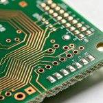
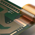
При разработке простых электронных устройств сложность — ваш злейший враг. A Двухслойная конструкция печатной платы обеспечивает идеальный баланс между экономичностью, простотой конструкции и скоростью производства для большинства базовых аппаратных решений. Независимо от того, создаете ли вы датчик для «умного дома» в рамках концепции Интернета вещей (IoT), простой драйвер светодиодов, модуль питания или учебный набор по электронике, понимание того, как эффективно использовать двухстороннюю печатную плату, позволит вам значительно сократить производственные затраты и существенно ускорить вывод продукта на рынок.
Что такое двухслойная конструкция печатной платы?
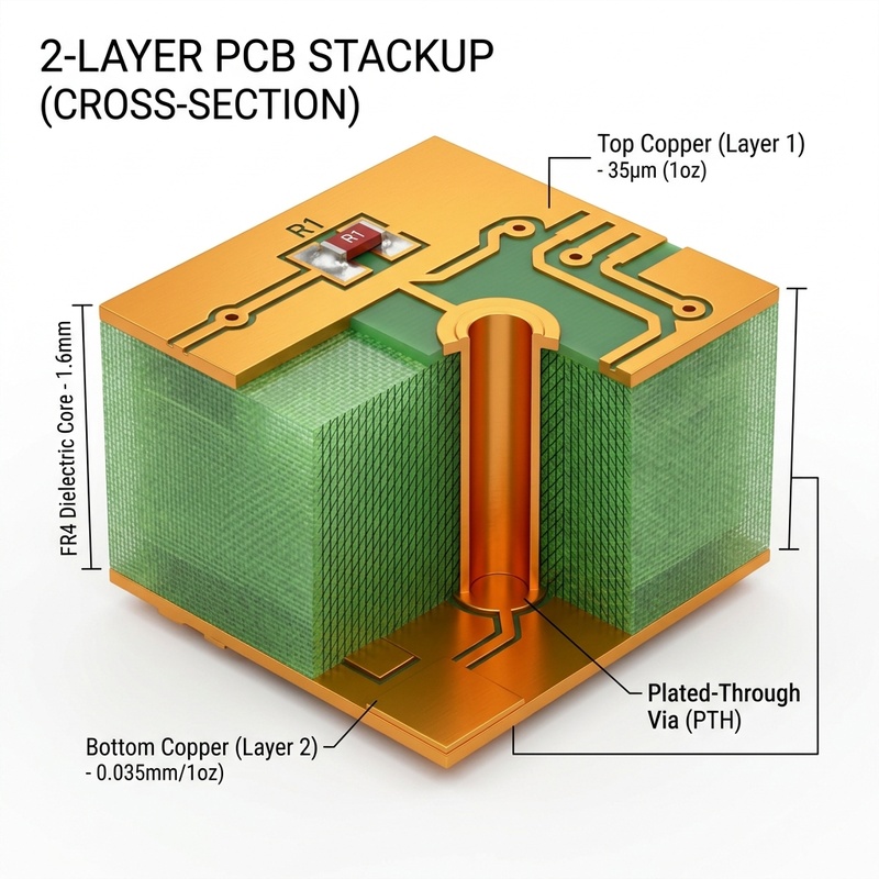
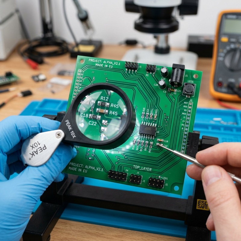
Двухслойная печатная плата, которую в отрасли обычно называют двусторонней, состоит ровно из двух слоев проводящей меди, разделенных жестким изолирующим диэлектрическим материалом — как правило, огнестойким стекловолокном, известным как FR4. В отличие от односторонних «голых» плат, которые ограничивают возможности трассировки, двухсторонние платы позволяют инженерам-аппаратчикам прокладывать электрические дорожки как на верхней, так и на нижней поверхности. Эти два проводящих слоя соединяются электрически с помощью металлизированных сквозных отверстий (PTH) или переходных отверстий.
Такая архитектура значительно повышает гибкость трассировки, позволяя размещать компоненты более компактно, не прибегая к сложным и дорогостоящим технологиям производства 4-слойных или 6-слойных печатных плат.
Основные компоненты двухсторонней печатной платы
Чтобы полностью понять процесс изготовления и оптимизировать файлы Gerber, необходимо знать, из каких слоёв состоит физическая конструкция от верха до низа:
- Паяльная маска и шелкография: Самый внешний защитный слой (обычно зелёного цвета, хотя выпускается и в других цветах), предотвращающий образование паяных мостиков при сборке; поверх него нанесена белая трафаретная краска с обозначениями компонентов и метками полярности.
- Верхний медный слой (слой 1): Обычно используется для размещения компонентов SMD (устройств поверхностного монтажа), прокладки критически важных высокоскоростных трасс передачи данных или прокладки основных линий электропитания.
- Диэлектрический сердечник из FR4: Конструктивная основа печатной платы. Она обеспечивает механическую жесткость и необходимую электрическую изоляцию между верхним и нижним медными слоями. Хотя стандартная толщина печатной платы часто составляет 1,6 мм, для более легких и компактных электронных устройств широко используются сердечники толщиной 0,8 мм или 1,2 мм.
- Нижний медный слой (слой 2): Часто используется в качестве выделенного сигнала обратный путь, широко распространённый способ заливки заземляющего слоя для экранирования от электромагнитных помех или для прокладки второстепенных сигналов, которые не поместились на основном верхнем слое.
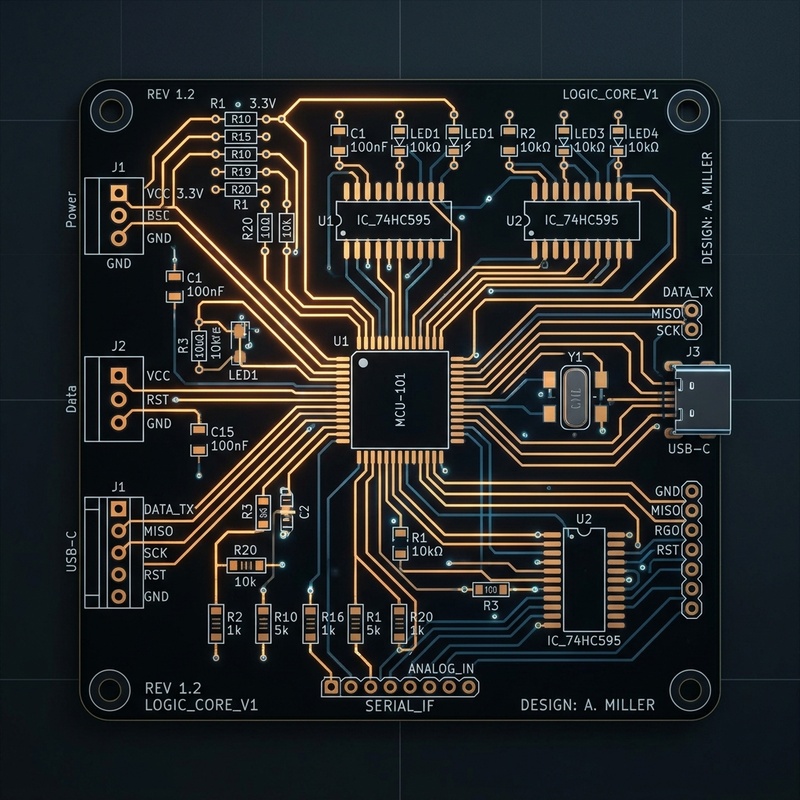
Почему для простых электронных устройств стоит выбирать двухслойную печатную плату?
Для приложений, в которых не используются цифровые сигналы с чрезвычайно высокой скоростью (такие как память DDR) или микропроцессоры с массивными корпусами BGA, двухслойная конструкция общепризнана как оптимальный вариант по ряду веских причин:
- Значительное сокращение затрат: Производство двухслойных плат обходится значительно дешевле, чем многослойных. Заводу-изготовителю не требуется проводить сложные процессы последовательного ламинирования или прессования сердечника.
- Снижение затрат на НРЭ: Расходы на единовременные инженерные работы (NRE), такие как затраты на изготовление инструментов и наладку, минимальны. Благодаря этому двухсторонние печатные платы идеально подходят для мелкосерийного производства.
- Сокращение сроков выполнения заказов: Двусторонние платы — это основной продукт в отрасли производства печатных плат. Практически любой стандартный производитель может изготовить их в короткие сроки — зачастую в течение 24–48 часов в случае экспресс-прототипирования.
- Упрощение создания прототипов и отладки: Благодаря тому, что все дорожки хорошо видны как сверху, так и снизу, проверка точек тестирования с помощью мультиметра или осциллографа, а также устранение неисправностей в прототипных платах становится невероятно простым делом.
Дополнительные аспекты: управление тепловым режимом и отделка поверхностей
Даже простые электронные устройства выделяют тепло. В двухслойной печатной плате теплоотвод в основном обеспечивается за счет использования больших медных заливок и термопроходные отверстия. Благодаря соединению верхней и нижней медных плоскостей с помощью массивов переходных отверстий, расположенных под нагревающимися компонентами (такими как стабилизаторы напряжения или драйверы двигателей), вся плата выступает в качестве пассивного радиатора.
Кроме того, крайне важно правильно выбрать вид отделки поверхности. Хотя HASL (выравнивание горячим воздушным припоем) является наиболее экономически эффективным стандартом для двухсторонних плат, ENIG (золото, погруженное в никель) Настоятельно рекомендуется использовать его, если в вашей простой электронике используются компоненты с мелким шагом, так как он обеспечивает идеально ровную поверхность для пайки.
Как спроектировать надёжную двухслойную печатную плату
Разработка надёжной двухслойной печатной платы требует строгой инженерной дисциплины. Поскольку у вас нет специального внутреннего плоскость земли, необходимо тщательно проложить трассы питания и заземления в программном обеспечении для проектирования электронных схем (например, Altium, KiCad или Eagle). Для успешной реализации аппаратного обеспечения выполните следующие важные шаги:
Шаг 1: Определите ширину и расстояние между дорожками
Прежде чем приступить к прокладке маршрута, рассчитайте необходимое ширина трассы исходя из максимального тока, который будет проходить по вашей схеме. Следуйте стандартным рекомендациям IPC-2221, чтобы обеспечить достаточное расстояние между дорожками и избежать коротких замыканий в процессе производства, особенно в зонах высокого напряжения.
Шаг 2: Грамотно проложить линии питания и заземления
Без внутренних плоскостей наземные контуры представляют собой самую серьезную угрозу для целостность сигнала и соответствие требованиям по электромагнитной совместимости (ЭМС). Старайтесь использовать толстые трассы заземления с низким импедансом или, что ещё лучше, разливка меди на нижнем слое, который выполняет функцию псевдо-заземляющей плоскости. Это способствует формированию путей обратного хода сигнала и снижает уровень электромагнитных помех (EMI).
Шаг 3: Обеспечить надлежащую развязку
Размещайте развязывающие и обходные конденсаторы как можно ближе к выводам питания микросхемы, насколько это физически возможно. Поскольку на двухслойной плате питающая дорожка может проходить по длинному участку с высокой индуктивностью, эти конденсаторы будут стабилизировать напряжение непосредственно на уровне компонентов.
Шаг 4: Проведите комплексную проверку DFM
Перед отправкой файлов Gerber в производственную компанию проведите проверку на технологичность (DFM). Убедитесь, что кольцевые зоны вокруг переходных отверстий имеют достаточный размер, чтобы предотвратить поломку сверла, а также что зазоры под паяльную маску находятся в пределах возможностей производителя.
Часто задаваемые вопросы (FAQ)
Можно ли прокладывать высокочастотные сигналы на двухслойной печатной плате?
Хотя с технической точки зрения это возможно для сигналов умеренной скорости (например, стандартных интерфейсов USB 2.0 или SPI), обеспечить стабильность сигнала чрезвычайно сложно управляемое сопротивление без надёжной, непрерывной опорной плоскости заземления. Для настоящих высокоскоростных конструкций и РЧ-приложений необходимо перейти на 4-слойная конструкция Настоятельно рекомендуется.
Какова стандартная толщина меди для двухслойной печатной платы?
Отраслевым стандартом является толщина медного слоя 1 унция (примерно 35 микрометров или 1,4 мил) как для верхнего, так и для нижнего слоя. Если ваш проект предусматривает использование силовой электроники, требующей высокой токопроводимости, вы можете заказать варианты изготовления с толщиной медного слоя 2 унции или даже более толстым слоем.
Обязательно ли наносить медную заливку с обеих сторон?
Хотя для простых низкочастотных схем это и не является строго необходимым, нанесение медного заземления как на верхний, так и на нижний слой (с их надежным соединением с помощью массивов переходных отверстий) значительно улучшает электромагнитное экранирование платы, снижает уровень шума и повышает эффективность теплоотвода.
Какие файлы необходимы для изготовления двухслойной печатной платы?
Вам потребуется экспортировать стандартный набор файлов Gerber (обычно используется формат RS-274X), отражающих медные слои, паяльную маску и шелкографию, а также файл NC Drill (формат Excellon), в котором указаны расположение и размеры всех переходных отверстий и сквозных отверстий.