Designing a printed circuit board (PCB) for high voltage applications presents unique challenges. Unlike low-voltage circuits, high voltage designs are susceptible to arcing, parasitic capacitance, and insulation breakdown if not properly managed. Among the most critical design parameters are clearance и creepage distances. Understanding and applying the correct high voltage PCB clearance rules is essential for ensuring product safety, reliability, and compliance with international standards such as IEC 60950 and IPC-2221.
What is PCB Clearance?
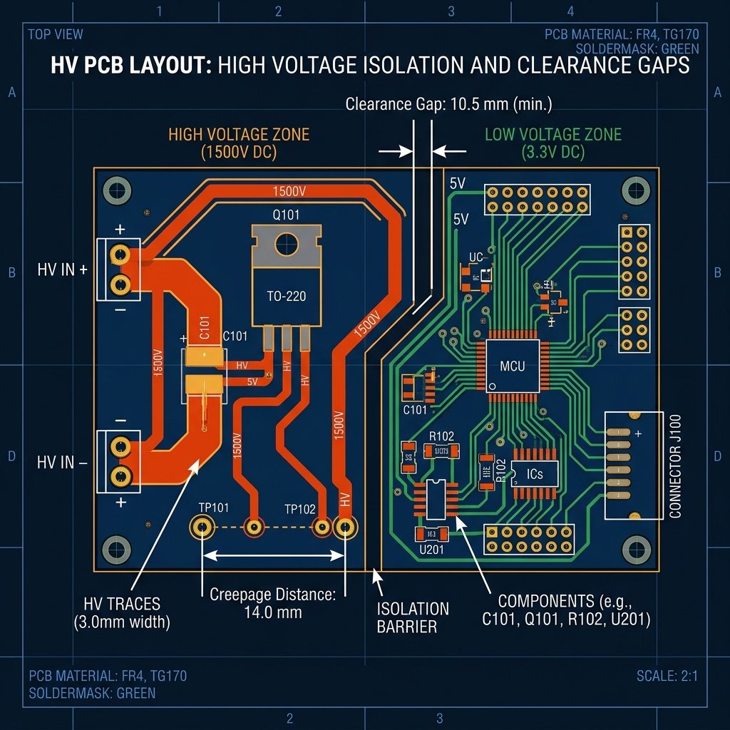
In the context of PCB design, clearance is defined as the shortest distance through the air between two conductive parts (like прокладки для деталей или медные следы). High voltage can cause air to ionize and become conductive, leading to an electrical arc between these conductors if they are too close. The breakdown voltage of air is approximately 3kV per millimeter, though this can vary significantly based on environmental factors like humidity, temperature, and atmospheric pressure.
When designing high voltage circuits, maintaining adequate PCB clearance prevents arcing. This is particularly crucial for safety-critical applications like medical devices, automotive electronics, and industrial power supplies. The required clearance depends not only on the peak working voltage but also on the operating environment and the pollution degree.
Creepage vs. Clearance: What is the Difference?
While clearance is the shortest distance through the air, creepage is the shortest distance along the surface of the insulating material (the PCB substrate) between two conductive parts. High voltage PCB clearance and creepage are related but distinct concepts.
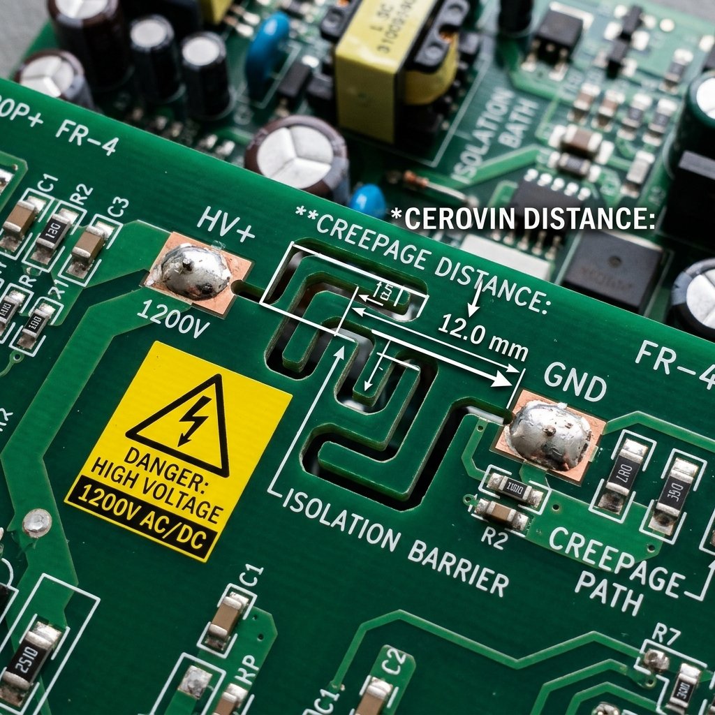
Creepage is critical because the surface of a PCB can become contaminated with dust, moisture, or other conductive particles over time (a concept measured by the pollution degree). These contaminants can create a conductive path across the dielectric surface, leading to a phenomenon known as tracking. Tracking can eventually carbonize the substrate, creating a permanent short circuit and posing a severe fire hazard.
Because creepage must follow the contours of the surface, it is always equal to or greater than the clearance distance. When the required creepage distance cannot be achieved on a flat board surface, designers often use techniques like milling slots or V-grooves between high voltage nodes to increase the surface distance without changing the physical layout.
Key Safety Standards for High Voltage PCB Design
Several international standards dictate the minimum high voltage PCB clearance and creepage requirements. Some of the most widely referenced standards include:
- IPC-2221: The generic standard on printed board design. It provides baseline tables for clearance and creepage based on voltage levels.
- IEC 60950-1 / IEC 62368-1: Standards for information technology and audio/video equipment. They focus heavily on user safety, separating hazardous high voltage circuits (primary) from low voltage user-accessible circuits (secondary).
- IEC 60664-1: Deals with insulation coordination for equipment within low-voltage systems. It introduces concepts like overvoltage categories and pollution degrees to determine clearance and creepage.
How to Design for High Voltage PCB Clearance
Follow these steps to ensure your PCB layout meets all high voltage clearance and creepage requirements.
Step 1: Determine the Peak Working Voltage
Identify the maximum continuous voltage across the insulation barrier. Be sure to consider both AC peak voltages and DC voltages. This is the foundational metric for calculating all spacing requirements.
Step 2: Identify the Pollution Degree and Overvoltage Category
Assess the operating environment. Pollution Degree ranges from 1 (clean, dry room) to 4 (outdoor, severe contamination). The Overvoltage Category (I to IV) defines the expected transient voltage spikes from the power grid. Higher degrees and categories require larger clearances.
Step 3: Consult the Applicable Standard Tables
Use standards like IPC-2221 or IEC 60950 to find the minimum required clearance and creepage values based on your voltage, pollution degree, and material group (CTI of the PCB substrate).
Step 4: Implement Routing Strategies and Slots
Route high voltage traces on internal layers where possible, as internal clearance rules are typically less stringent. If surface creepage is insufficient, add isolation slots (routed cutouts) between the high voltage pads to artificially increase the surface distance.

Advanced Techniques for Managing High Voltage
In addition to strict adherence to spacing rules, high voltage PCB designers utilize several advanced techniques to enhance safety and performance:
- Material Selection (CTI): The Comparative Tracking Index (CTI) measures a material’s resistance to surface tracking. Materials with a higher CTI allow for smaller creepage distances. Using specialized high-CTI FR4 or polyimide can be beneficial.
- Конформное покрытие: Applying an insulating conformal coating over the assembled PCBA can significantly reduce the required clearance and creepage distances by protecting the surface from moisture and contamination.
- Avoid Sharp Corners: High voltage tends to arc more easily from sharp points due to high electric field concentration. Always use rounded pads and smooth, curved traces for high voltage nodes.
Часто задаваемые вопросы
What is the rule of thumb for PCB clearance?
A common, very conservative rule of thumb for standard environments is to allow for 1 mm of clearance for every 100V. However, this is not a substitute for consulting proper standards like IPC-2221, especially above 500V or in contaminated environments.
How do slots improve creepage distance?
Slots improve creepage distance because the current must travel down into the slot, across the bottom, and back up the other side, effectively lengthening the surface path between two points without changing their physical straight-line separation on the board.
Does conformal coating replace the need for clearance?
No, conformal coating does not entirely replace the need for clearance. While it can reduce the required spacing by protecting against environmental pollution, base clearance rules must still be followed to prevent dielectric breakdown of the coating itself under high electric fields.
Mastering high voltage PCB clearance is a non-negotiable skill for modern electronics designers. By understanding the distinction between clearance and creepage, rigorously applying industry standards, and utilizing smart routing techniques, you can ensure your designs are both safe and highly reliable.