В сфере современной электроники проектирование печатных плат (PCB) приобретает как никогда ранее решающее значение. По мере того как устройства становятся все меньше, быстрее и сложнее, обеспечение стабильной подачи питания становится одной из главных задач для инженеров. В основе этой задачи лежит проектирование плоскости питания. Оптимально спроектированная плоскость питания необходима для стабильного распределения напряжения, минимизации электромагнитных помех (ЭМП) и поддержания целостности сигнала по всей плате.
При проектировании печатных плат с высокой скоростью работы или высокой плотностью размещения компонентов необходимо тщательно планировать сеть подачи питания (PDN). PDN охватывает все, начиная от модуля стабилизации напряжения (VRM) и заканчивая интегральными схемами (ИС), потребляющими энергию. Планы питания выступают в качестве основных каналов передачи этой энергии. Если планы питания спроектированы неверно, напряжение, поступающее на компоненты, может колебаться, что приводит к непредсказуемому поведению, повреждению данных или полному отказу системы.

Понимание роли силовых плоскостей
План питания — это слой меди на печатной плате, полностью предназначенный для одного напряжения питания (например, 3,3 В, 5 В или 12 В). Использование сплошного плана вместо прокладки питающих дорожек дает ряд явных преимуществ. Во-первых, это значительно снижает сопротивление постоянному току между источником питания и нагрузкой. Такое низкое сопротивление сводит к минимуму падения напряжения, обеспечивая подачу правильного уровня напряжения на удалённые компоненты даже при высоких токовых нагрузках.
Во-вторых, плоскости питания в сочетании с прилегающими заземляющими плоскостями образуют большую распределенную ёмкость. Эта межплоскостная ёмкость весьма эффективно подаёт высокочастотные переходные токи на импульсные компоненты, снижая уровень шума на шине питания. Кроме того, сплошные плоскости обеспечивают превосходную обратный путь для высокочастотных сигналов, что имеет решающее значение для снижения индуктивности контура и уменьшения электромагнитных помех.
Основные стратегии оптимизации
Оптимизация конструкции силовой схемы требует комплексного подхода. Ниже приведены некоторые из наиболее важных факторов, которые необходимо учитывать для обеспечения стабильного распределения напряжения.
1. Структура стратегических слоев
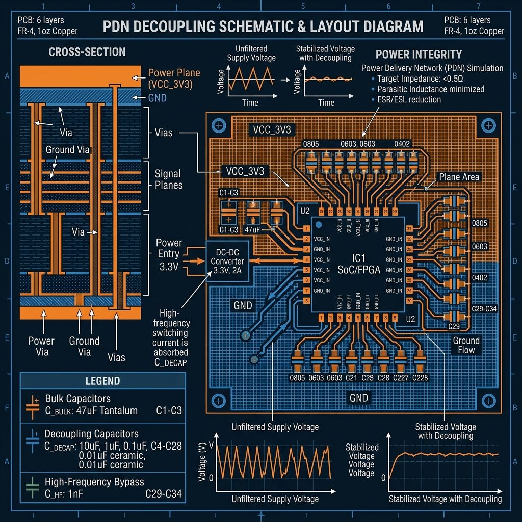
Расположение слоёв в вашем Структура печатной платы является основой качественного проектирования PDN. В идеале, питание и наземные плоскости должны располагаться как можно ближе друг к другу. Чем ближе они находятся, тем выше межплоскостная ёмкость и тем ниже индуктивность. В высокочастотных схемах для максимального использования этого преимущества обычно применяют тонкие диэлектрики (например, толщиной 2–4 мил) между слоями питания и заземления.
2. Эффективное размещение развязывающих конденсаторов
В то время как межплоскостная ёмкость позволяет работать на очень высоких частотах, дискретные развязывающие конденсаторы необходимы для низко- и среднечастотного диапазона. Расположение этих конденсаторов имеет решающее значение. Их следует размещать как можно ближе к выводам питания микросхем, насколько это физически возможно, чтобы свести к минимуму индуктивность трасс и переходных отверстий, соединяющих их. Использование конденсаторов с различными номиналами (например, 0,1 мкФ, 1 мкФ, 10 мкФ) обеспечивает низкий импеданс в широком частотном диапазоне.
3. Сведение к минимуму перфораций плоскости
Переходные отверстия, проходящие через плоскость питания или заземления, образуют отверстия, или “анти-пады”, в медном слое. Если слишком много переходных отверстий размещено близко друг к другу (например, при плотной разводке BGA), эти анти-пады могут сливаться, образуя большую пустоту или щель в плоскости. Эта щель заставляет токи обратного хода проходить более длинный путь вокруг препятствия, что значительно увеличивает индуктивность контура и может привести к проблемам с электромагнитными помехами (EMI). Для сохранения целостности плоскостей необходимо тщательно прокладывать трассы переходных отверстий и соблюдать надлежащие расстояния между ними.
4. Разделенные плоскости и несколько напряжений
Многие современные печатные платы требуют наличия нескольких напряженных шин. Когда на одном слое необходимо разместить линии с разными напряжениями, плоскость разделяется на отдельные медные островки. При разделении плоскостей крайне важно обеспечить, чтобы высокоскоростные сигналы не пересекали место раздела на соседних слоях. Пересечение раздела прерывает непрерывный путь возврата, что приводит к серьезным проблемам с целостностью сигнала. Если сигнал должен пересекать раздел, следует использовать соединительные конденсаторы для обеспечения пути возврата переменного тока.
Тепловые аспекты при проектировании силовой платы
Стабильное распределение напряжения связано не только с электрическими характеристиками, но и с управлением тепловым режимом. Сильные токи, протекающие по плоскостям питания, выделяют тепло. Если это тепло не распределяется и не отводится эффективно, могут возникать локальные зоны повышенной температуры, что со временем может привести к повреждению компонентов или снижению надежности платы.
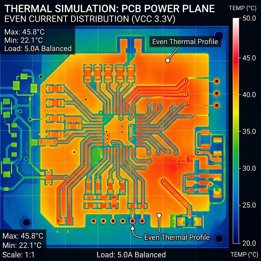
Использование более толстой меди (например, 2 унции или более) для плоскостей питания снижает сопротивление постоянному току и, следовательно, уменьшает резистивное нагревание (потери I²R). Кроме того, сплошная медная поверхность служит отличным теплораспределителем, отводящим тепло от высокомощных компонентов, таких как стабилизаторы напряжения и процессоры. На этапе проектирования часто используются тепловые симуляции для выявления потенциальных «горячих точек» и проверки того, что заливка меди и тепловые переходные отверстия соответствуют ожидаемым мощностным нагрузкам.
Раздел «Как работать с микроданными»
Как спроектировать оптимизированную плоскость питания
Пошаговое руководство по настройке плоскости мощности для обеспечения максимальной стабильности и производительности.
Шаг 1: Определение структуры слоев
Определите необходимое количество слоев и расположите плоскости питания в непосредственной близости от плоскостей заземления, чтобы максимально увеличить межплоскостную ёмкость.
Шаг 2: Планирование подачи электроэнергии
Определите все необходимые области напряжения и спланируйте медные отливки или плоскость разделяется соответствующим образом. Избегайте сложных форм, напоминающих лабиринт.
Шаг 3: Тщательно прокладывайте переходные отверстия
Располагайте переходные отверстия на достаточном расстоянии друг от друга, чтобы их антиконтактные площадки не соединялись и не образовывали щели в плоскости, что нарушает пути обратного тока.
Шаг 4: Установка развязывающих конденсаторов
Размещайте развязывающие конденсаторы непосредственно рядом с выводами питания важных микросхем, чтобы свести к минимуму индуктивность трасс.
Раздел «Микроданные» на странице часто задаваемых вопросов
Часто задаваемые вопросы
Почему межплоскостная ёмкость имеет важное значение?
Межплоскостная ёмкость, образующаяся за счёт близко расположенных друг к другу плоскостей питания и заземления, является отличным источником высокочастотного заряда, стабилизирующим напряжение при быстрых переключениях и более эффективно подавляющим высокочастотные помехи, чем отдельные конденсаторы.
Что произойдет, если высокочастотный сигнал пересечет разъем в плоскости питания?
Когда трасса сигнала пересекает зазор или разрыв в своей опорной плоскости, путь обратного тока прерывается. Обратный ток вынужден идти более длинным путем, что увеличивает площадь контура, а это приводит к росту индуктивности, ухудшению качества сигнала и усилению электромагнитных помех.
Какой толщины должна быть медь для силового плана?
Требуемая толщина медного слоя зависит от предполагаемой силы тока. Стандартный слой меди толщиной 1 унция (1,4 мил) зачастую достаточен для низких и умеренных значений силы тока. Для высокомощных систем может потребоваться слой меди толщиной 2 или даже 3 унции, чтобы свести к минимуму сопротивление и выделение тепла.
В заключение следует отметить, что оптимизация конструкции силовой схемы является одним из ключевых аспектов создания надёжных и высокопроизводительных электронных устройств. Тщательно продумывая последовательность слоёв, размещение компонентов, пути обратного тока и систему теплоотвода, инженеры могут обеспечить стабильное распределение напряжения, отвечающее высоким требованиям современных конструкций печатных плат.