Im Bereich des Designs von Hochgeschwindigkeits-Leiterplatten (PCB), Signalintegrität ist von größter Bedeutung. Einer der wichtigsten Aspekte zur Wahrung dieser Integrität ist die effektive Gestaltung des Rückleitungspfads auf der Leiterplatte. Eine mangelhafte Planung des Rückleitungspfads kann zu einer Vielzahl von Problemen führen, insbesondere zu Übersprechen, elektromagnetischen Störungen (EMI) und Ground-Bounce. Dieser umfassende Leitfaden befasst sich eingehend damit, was der Rückleitungspfad ist, warum er wichtig ist und wie Sie ihn optimieren können, um Übersprechen zu beseitigen und eine robuste Leistung in Ihren elektronischen Schaltungen sicherzustellen.
Den Rückleitungspfad auf der Leiterplatte verstehen
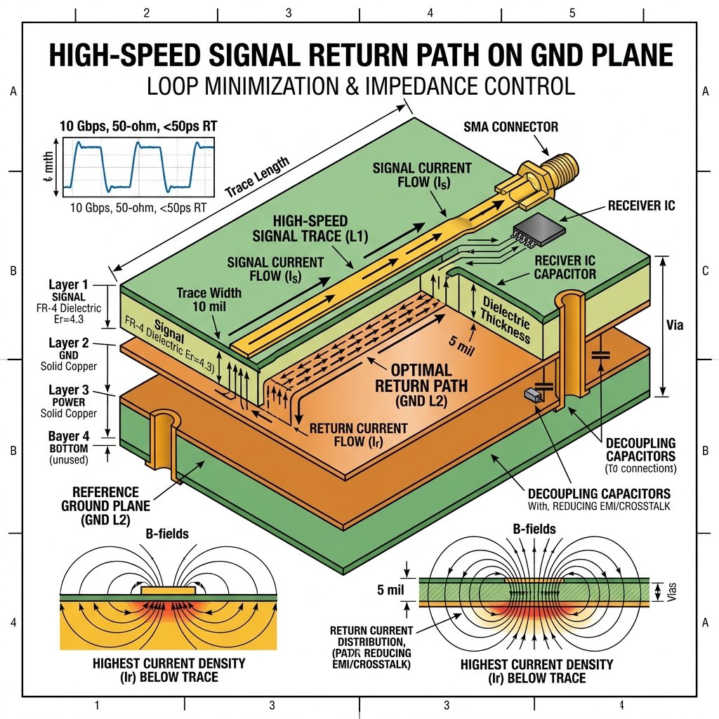
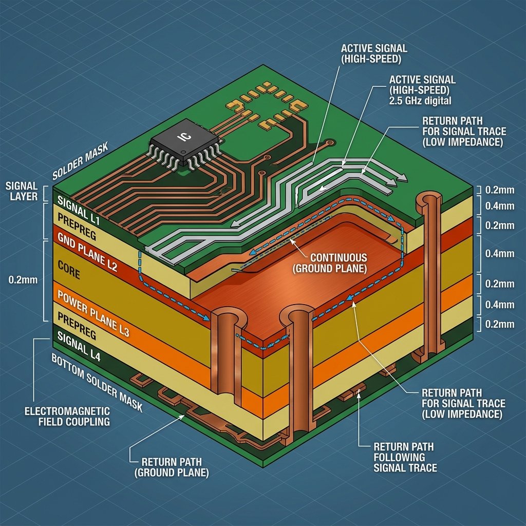
Jedes elektrische Signal verläuft in einer geschlossenen Schleife. Während Entwickler viel Zeit damit verbringen, den Vorwärtspfad (die Signalleitung) sorgfältig zu verlegen, wird der Rückweg oft dem Zufall überlassen oder man geht davon aus, dass er sich von selbst regelt, indem man einfach alles an eine Grundplatte. Der Rückweg ist der Weg, den der Strom nimmt, um zu seiner Quelle zurückzukehren. Bei niederfrequenten Signalen folgt der Rückstrom dem Weg des geringsten Widerstands. Bei Hochfrequenzsignale, der Rückstrom wählt den Weg des geringsten Impedanz, die sich in der Regel direkt unterhalb der Signalleitung auf der nächstgelegenen Referenzebene befindet.
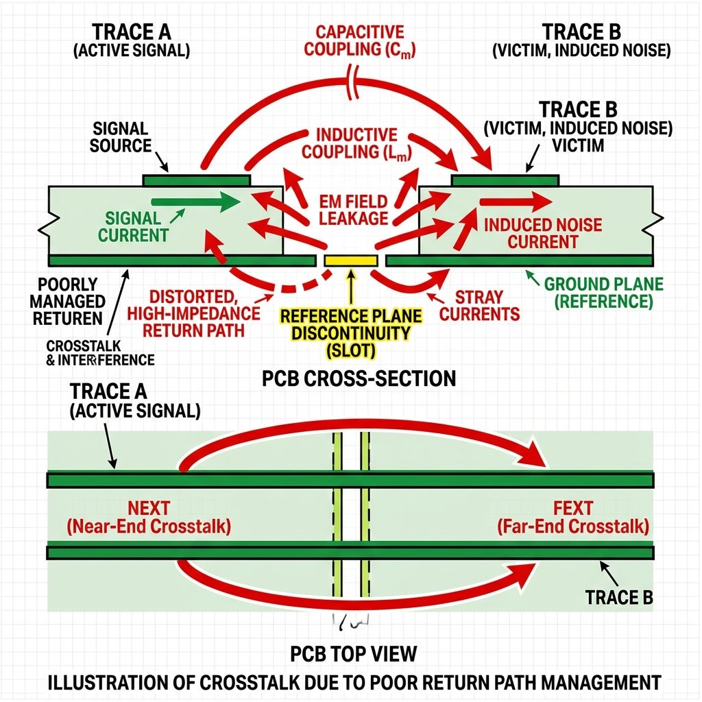
Wenn der Rückleitungsweg unterbrochen wird – durch eine geteilte Ebene, einen Spalt oder durch Übergänge ohne angrenzende Masse-Vias –, muss der Rückstrom einen alternativen Weg finden. Diese größere Schleifenfläche erhöht die Induktivität und führt dazu, dass sich das Signal mit benachbarten Leiterbahnen koppelt, was zu Übersprech- und EMI-Problemen führt.
Der Zusammenhang zwischen Rückkanal und Übersprechen
Übersprechen tritt auf, wenn das elektromagnetische Feld einer Leiterbahn (dem „Störer“) eine unerwünschte Spannung oder einen unerwünschten Strom auf einer angrenzende Leiterbahn (das Opfer). Die Stärke dieser Kopplung ist direkt proportional zur Schleifenfläche sowohl des Aggressor- als auch des Opfersignals.
Verfügt ein Signal über einen durchgehenden Rückleitungspfad direkt unterhalb der Leiterbahn, werden die elektromagnetischen Felder eng zwischen der Leiterbahn und der Referenzebene eingeschlossen. Diese enge Kopplung minimiert die Streufelder, die benachbarte Leiterbahnen stören könnten. Ist der Rückleitungspfad hingegen unterbrochen, breiten sich die Felder aus und suchen nach einem Weg zurück zur Quelle, wodurch die Wahrscheinlichkeit einer Kopplung mit anderen Signalen erheblich steigt. Daher ist die Bereitstellung eines ununterbrochenen, niederohmigen Rückleitungswegs der effektivste Weg, um Übersprechen zu beseitigen.
So optimieren Sie den Rückpfad auf der Leiterplatte
Schritt-für-Schritt-Anleitung zur Verwaltung des Rückleitungspfads auf der Leiterplatte
Befolgen Sie bei der Layout-Erstellung diese systematischen Schritte, um durchgehende Rückleiter zu gewährleisten und Übersprechen zu minimieren.
Schritt 1: Kritische und Hochgeschwindigkeitssignale identifizieren
Schritt 2: Benachbarte zusammenhängende Referenzebenen zuweisen
Schritt 3: Vermeiden Sie die Verlegung über Trennebenen
Schritt 4: Gehen Sie bei der Verwaltung von Ebenenübergängen sorgfältig vor
Fortgeschrittene Aspekte bei Mixed-Signal-Entwürfen
Bei Mixed-Signal-Schaltungen, bei denen sowohl analoge als auch digitale Schaltungen auf derselben Platine untergebracht sind, wird die Steuerung des Rückleitungspfads noch komplexer. Digitale Rückströme enthalten hochfrequentes Rauschen, das empfindliche analoge Signale erheblich beeinträchtigen kann, wenn sie denselben Rückleitungspfad nutzen.
Der traditionelle Ansatz bestand darin, die Masseflächen physisch in analoge und digitale Bereiche aufzuteilen. Moderne Best Practices tendieren jedoch dazu, eine einzige, einheitliche Masseebene zu verwenden und die Anordnung der Bauteile sorgfältig zu unterteilen. Indem analoge Bauteile in einem Bereich und digitale Bauteile in einem anderen platziert werden und sichergestellt wird, dass keine digitalen Leiterbahnen in den analogen Bereich übergreifen, trennen sich die jeweiligen Rückströme auf natürliche Weise voneinander und verbleiben unter ihren Quellleiterbahnen, ohne dass es zu einer gegenseitigen Beeinflussung kommt.
Häufig gestellte Fragen
Warum folgt der Rückweg dem Pfad mit der geringsten Impedanz?
Kann ich eine Stromleitung als Rückleitung nutzen?
Was passiert, wenn ich beim Wechseln der Ebenen eine Verbindungsbohrung vergesse?
Schlussfolgerung
Bei der Entwicklung einer leistungsstarken Leiterplatte muss dem Rückleitungspfad dieselbe Sorgfalt und Aufmerksamkeit gewidmet werden wie der Signalleitung selbst. Durch die Gewährleistung durchgehender Referenzebenen, die Vermeidung von Unterbrechungen und die ordnungsgemäße Gestaltung von Schichtübergängen mit Verbindungsvias können Sie die elektromagnetischen Felder eng koppeln. Dies minimiert nicht nur die elektromagnetische Störung (EMI), sondern beseitigt auch grundlegend die Ursachen für Übersprechen, was zu einem saubereren, zuverlässigeren und robusteren elektronischen Produkt führt.