Optimierung der Durchkontaktierung bei Leiterplatten für zuverlässige Verbindungen
Einleitung
In the fast-paced and highly complex world of modern electronics, ensuring seamless and uninterrupted conductivity across multiple layers of a printed circuit board is paramount. The sophisticated technique of perfecting pcb through hole plating stands as a critical pillar in achieving this ambitious goal. This transformative process turns non-conductive, mechanically drilled holes into highly reliable electrical pathways. By doing so, it connects different layers of the board and provides robust mechanical support for both surface mount and through-hole components. As smart devices become progressively smaller and industrial electronics grow more complex, mastering this intricate technique is absolutely essential for any high-quality PCB manufacturing process. Without flawless plating, the structural and electrical integrity of the entire assembly is put at risk.
The Essential Role of Plated Through-Holes (PTH)
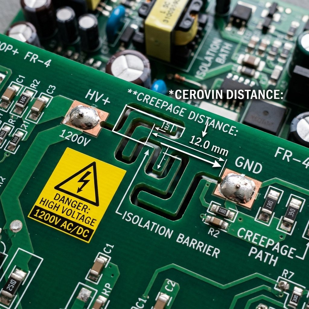
Plated through-holes (PTH) are considerably more than just simple conductive vias; they act as the essential lifelines of advanced multi-layer printed circuit boards. When manufacturers focus their efforts on perfecting pcb through hole processes, they can guarantee that both high-speed signals and significant power loads travel efficiently across layers without degradation, signal loss, or unwanted resistance build-up. A well-plated and uniform hole ensures maximum structural integrity, which is particularly vital when components are continuously subjected to extreme thermal stress during soldering or severe mechanical vibration in the field. This level of durability is critically important in demanding and advanced applications, such as the production of rigid-flex PCBs, where maintaining reliability under constant dynamic and flexible conditions is non-negotiable for the end-user.
Conversely, failing to achieve a consistent and uniform plating thickness can lead to a host of catastrophic defects. These include plating voids, barrel cracks, or even complete electrical opens, all of which result in extremely costly factory reworks and severely compromised end-products. Therefore, rigorous and unyielding attention to detail during every single phase of the plating process is essential for ensuring long-term product reliability and customer satisfaction.
The Step-by-Step Process for Perfecting PCB Through Hole Plating
Achieving the perfect plated through-hole is not a simple task; it involves a meticulously controlled and closely monitored sequence of complex chemical and electrochemical steps. Here is an in-depth look at how top-tier manufacturers ensure reliable connections.
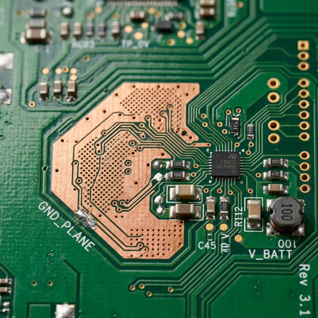
1. Precision Drilling and Thorough Desmearing
The journey begins with highly precise mechanical or laser drilling of the required vias. Following this intense drilling phase, the “smear”—a thin layer of melted epoxy resin caused by the extreme heat and friction of the drill bit—must be completely removed. The desmearing process usually involves aggressive permanganate chemical baths or plasma treatments designed to clean the hole walls thoroughly, preparing the exposed inner layers for the subsequent plating steps. Ensuring an impeccably clean surface is the first, and arguably most critical, step in perfecting pcb through hole connections.
2. Electroless Copper Deposition
Since the fiberglass substrate and epoxy resin inside the freshly drilled hole are inherently non-conductive, a very thin layer of copper must be deposited chemically rather than electrically. This specific electroless copper process evenly coats the entire inner wall of the microscopic hole. By doing so, it creates a crucial micro-thin, conductive base layer that sets the stage and allows for the much thicker electroplating process to follow.
3. Advanced Electroplating
Once the initial, delicate conductive layer is fully established, the entire board is immersed into electrolytic copper plating baths. Here, a much thicker and more robust layer of copper is electrochemically deposited directly onto the hole walls to achieve the required final thickness and structural integrity. This step demands the strictest control of electrical current density, fluid agitation, and precise chemical bath composition to guarantee a perfectly uniform plating thickness from top to bottom.
4. Comprehensive Quality Inspection and Testing
The final, indispensable step involves highly rigorous PCB quality control measures. Cross-sectional microsections of the plated holes are carefully extracted and meticulously examined under high-powered microscopes to scientifically verify plating thickness, wall uniformity, and the total absence of any microscopic voids or barrel cracks. In addition, exhaustive automated electrical testing (like flying probe testing) is performed to definitively confirm 100% connectivity and isolation.
Overcoming Common Challenges in Plating Operations
Even when utilizing the most advanced technology, the goal of perfecting pcb through hole plating routinely presents significant manufacturing challenges. One incredibly common and difficult issue is “throwing power.” This term refers to the chemical solution’s ability to consistently plate the exact center of a deep hole to the very same thickness as the outer surface. High aspect ratio holes (scenarios where the total depth of the hole is drastically greater than its diameter) require highly specialized chemical plating solutions and advanced pulse plating techniques to successfully overcome this fluid dynamics challenge. Additionally, ensuring seamless compatibility with various final PCB surface finishes is absolutely necessary to prevent long-term copper oxidation and to guarantee excellent, defect-free solderability during the ultimate assembly phase.
Häufig gestellte Fragen
Why is perfecting PCB through hole plating so critically important?
Perfecting PCB through hole plating is absolutely vital because these plated holes provide the fundamental electrical connections between the many different layers of a complex multi-layer board. Poor plating can immediately lead to unexpectedly high resistance, frustrating intermittent connections, or complete, disastrous circuit failure, ultimately compromising the entire electronic device and leading to field failures.
What are the primary causes of voids in through-hole plating?
Plating voids are typically caused by microscopic air bubbles becoming trapped in the hole during the wet plating process, completely inadequate desmearing that leaves resin residue, or harmful impurities and imbalances in the chemical plating baths. These voids represent critical weak spots where electrical conductivity is severely reduced and structural strength is fatally compromised.
How thick should the copper plating ideally be inside a standard through-hole?
The widely accepted industry standard thickness for through-hole copper plating is generally around 1 mil (which is equivalent to 25.4 micrometers). This specific thickness is usually enough to ensure adequate conductivity and necessary mechanical strength for most commercial applications. However, high-reliability and mission-critical applications (such as those found in the aerospace, medical, or automotive sectors) will frequently require significantly thicker plating to withstand extreme environments.