Der Entwurf einer 4-lagigen Leiterplatte (PCB) ist in der modernen Elektronik eine gängige Anforderung. Wenn Ihre Schaltung für eine einfache 2-lagige Leiterplatte zu komplex wird oder wenn Sie eine bessere Signalintegrität und bei der Stromverteilung ist der Übergang zu einem 4-lagigen Leiterplattenaufbau der logische nächste Schritt. Eine standardmäßige 4-lagige Leiterplatte besteht aus einer Deckschicht, einer Grundschicht und zwei Zwischenlagen, die in der Regel als Strom- und Masseflächen dienen.
In diesem umfassenden Leitfaden führen wir Sie durch den gesamten Prozess der Entwicklung eines robusten und zuverlässigen 4-lagigen Leiterplattenaufbaus. Wir behandeln dabei die Standardkonfigurationen, Vorteile und wichtigsten Aspekte, die Sie beachten müssen, um sicherzustellen, dass Ihr Entwurf fertigungsfähig ist und eine optimale Leistung erbringt.
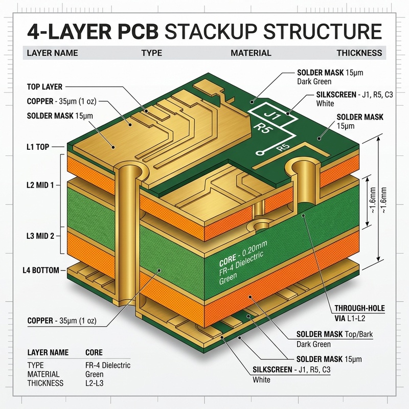
Das 4-lagige Leiterplatten-Stackup verstehen
Bevor wir uns mit den einzelnen Entwurfsschritten befassen, ist es wichtig zu verstehen, was ein 4-lagiger Leiterplatten-Stackup eigentlich ist. Ein Stackup bezeichnet die Anordnung der Kupfer- und Isolierschichten, aus denen eine Leiterplatte vor dem Layout-Entwurf besteht. Ein gut konzipierter Stackup kann elektromagnetische Emissionen und Übersprechen minimieren und die Signalintegrität der Leiterplatte verbessern.
Die gängigste Konfiguration für eine 4-lagige Leiterplatte lautet: Signal / Masse / Stromversorgung / Signal. Diese Anordnung bietet hervorragende Rückleitungswege für Hochgeschwindigkeitssignale und reduziert elektromagnetische Störungen (EMI). Die inneren Schichten dienen als Abschirmung für die Signale auf den äußeren Schichten, weshalb diese Konfiguration für die meisten Standardanwendungen dringend empfohlen wird.
So entwirft man einen 4-lagigen Leiterplattenaufbau
Befolgen Sie diese Schritte, um einen standardmäßigen 4-lagigen Leiterplattenaufbau für Ihr nächstes Elektronikprojekt sorgfältig zu planen und umzusetzen.
Schritt 1: Legen Sie die Anordnung der Schichten fest
Der erste Schritt besteht darin, zu entscheiden, wofür die einzelnen Schichten verwendet werden sollen. Wie bereits erwähnt, lautet der Standard „Signal-Masse-Stromversorgung-Signal“. Bei einigen Mixed-Signal-Designs kann man sich jedoch für „Masse-Signal-Signal-Masse“ entscheiden, wenn hochsensible Leiterbahnen vorhanden sind, auch wenn dies die Stromversorgung verkompliziert. Halten Sie sich an den Standard „Signal-GND-VCC-Signal“, es sei denn, Sie haben einen konkreten Grund, davon abzuweichen.
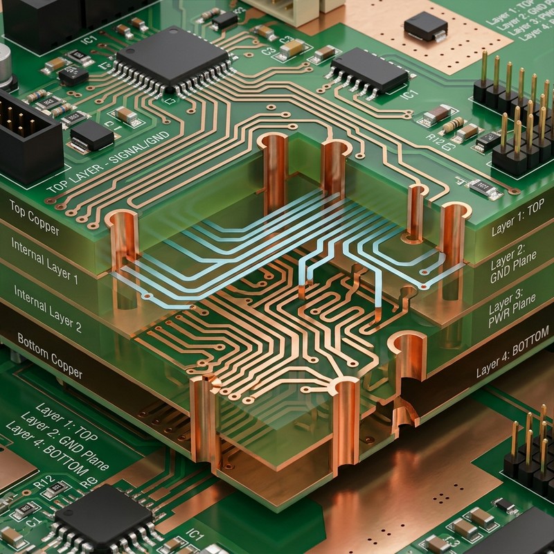
Schritt 2: Berechnung der Impedanzanforderungen
Wenn Ihre Platine über Hochgeschwindigkeitsschnittstellen wie USB, HDMI oder PCIe verfügt, benötigen Sie angepasste Impedanz. Erfragen Sie bei Ihrem Leiterplattenhersteller die Standardangaben zum 4-lagigen Schichtaufbau, einschließlich der Kerndicke, der Prepreg-Dicke und der Dielektrizitätskonstanten. Geben Sie diese Werte in einen Impedanzrechner ein, um die Leiterbahnbreiten und -abstände zu ermitteln.
Schritt 3: Verlegen der Strom- und Masseflächen
Die internen Ebenen sollten so weit wie möglich aus massivem Kupfer bestehen. Bei der Aufteilung von Ebenen (beispielsweise bei mehreren Spannungsbereichen wie 3,3 V und 5 V) ist darauf zu achten, dass keine Hochgeschwindigkeitssignale über die Trennstellen auf den angrenzenden Signalschichten verlegt werden. Das Überqueren einer geteilten Ebene stört die Rückweg und verursacht erhebliche EMI-Probleme.

Schritt 4: Fanout und Bauteilplatzierung
Sobald die Versorgungs- und Masseflächen angelegt sind, beginnen Sie mit der Platzierung Ihrer Bauteile. Platzieren Sie Entkopplungskondensatoren so nah wie möglich an den Versorgungsanschlüssen Ihrer ICs und legen Sie eine Durchkontaktierung direkt zu den Versorgungs- und Masseflächen an. Dies minimiert die Schleifeninduktivität und gewährleistet eine saubere Stromversorgung Ihrer empfindlichen Bauteile.
Schritt 5: Signalebenen verlegen
Leiten Sie Ihre Signale schließlich auf der obersten und untersten Schicht. Halten Sie Hochgeschwindigkeitssignale so kurz wie möglich und vermeiden Sie unnötige Schichtwechsel. Wenn ein Schichtwechsel unvermeidbar ist, versuchen Sie, in der Nähe eine Masse-Via anzubringen, um einen durchgehenden Rückweg für den Signalstrom zu gewährleisten.
Häufige Fallstricke beim Entwurf von 4-lagigen Leiterplatten
Selbst erfahrene Entwickler können beim Übergang zu mehrschichtigen Leiterplatten Fehler machen. Ein häufiger Fehler ist das Ignorieren des Rückleitungswegs von Signalen. Hochfrequente Signale folgen dem Weg mit der geringsten Induktivität, der sich direkt unterhalb der Leiterbahn auf der nächstgelegenen Referenzebene befindet. Ist diese Referenzebene unterbrochen oder zu weit entfernt, strahlt das Signal Störsignale ab.
Eine weitere Falle ist eine unzureichende Entkopplung. Da eine 4-lagige Leiterplatte oft eine erhebliche Kapazität zwischen den eng beieinander liegenden Stromversorgungs- und Masseebenen aufweist (sofern sie so konfiguriert ist), gehen Entwickler manchmal davon aus, dass weniger Entkopplungskondensatoren benötigt werden. In der Standardkonfiguration „Signal-GND-PWR-Signal“ sind die Ebenen jedoch in der Regel durch einen dicken Kern voneinander getrennt, wodurch die Kapazität zwischen den Ebenen sehr gering ist. Man muss sich daher weiterhin auf lokale Entkopplungskondensatoren verlassen.
Häufig gestellte Fragen zu 4-lagigen Leiterplatten
Wie dick ist eine 4-lagige Leiterplatte in der Regel?
Die gängigste Standarddicke für eine 4-lagige Leiterplatte beträgt 1,6 mm (0,063 Zoll). Je nach Ihren spezifischen Anforderungen und Vorgaben können Hersteller jedoch Leiterplatten mit Dicken von 0,4 mm bis zu 3,2 mm herstellen.
Wie viel kostet eine 4-lagige Leiterplatte im Vergleich zu einer 2-lagigen?
Im Allgemeinen kostet eine 4-lagige Leiterplatte etwa 50% bis 100% mehr als eine 2-lagige Leiterplatte gleicher Größe und Menge. Dies ist auf die zusätzlichen Laminierungsschritte und Materialien zurückzuführen, die erforderlich sind, um die verschiedenen Lagen miteinander zu verbinden.
Kann ich Bauteile auf beiden Seiten einer 4-lagigen Leiterplatte anbringen?
Ja, Sie können Bauteile problemlos sowohl auf der obersten als auch auf der untersten Schicht einer 4-lagigen Leiterplatte platzieren. Dies ist bei Designs mit hoher Bauteildichte gängige Praxis. Sie verwenden einfach Durchkontaktierungen, um die Bauteile mit den internen Versorgungs- und Masseebenen zu verbinden oder Signale zwischen den äußeren Schichten zu leiten.
Schlussfolgerung
Das Entwerfen eines 4-lagigen Leiterplatten-Stackups ist eine unverzichtbare Kompetenz für jeden Elektronikingenieur. Wenn Sie sich an die Standardkonfigurationen halten und die Signalintegrität im Blick behalten, können Sie Leiterplatten entwickeln, die zuverlässig und rauscharm sind und sich für die Serienfertigung eignen. Denken Sie immer daran, sich bereits früh im Entwurfsprozess mit Ihrem Leiterplattenhersteller abzustimmen, um sicherzustellen, dass Ihre Entscheidungen zum Schichtaufbau mit dessen Fertigungsmöglichkeiten vereinbar sind.