Bei der Entwicklung moderner Elektronik ist es oft erforderlich, erhebliche Rechenleistung auf unglaublich kleiner Baufläche unterzubringen. Da die Bauteildichte und die Signalgeschwindigkeit zunehmen, muss sich die zugrunde liegende Leiterplatte (PCB) weiterentwickeln, um diesen Anforderungen gerecht zu werden. Für viele Hochleistungsanwendungen reicht eine standardmäßige 4- oder 6-lagige Leiterplatte einfach nicht aus. Hier kommt der robuste und leistungsstarke 10-lagige Leiterplattenaufbau ins Spiel.
Der Aufbau einer 10-lagigen Leiterplatte
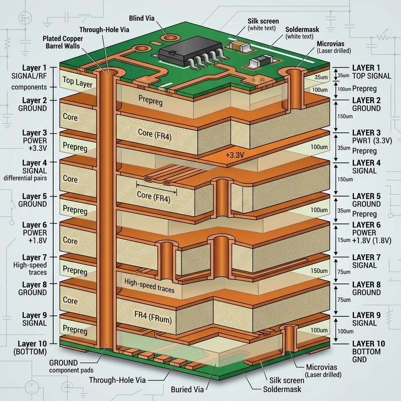
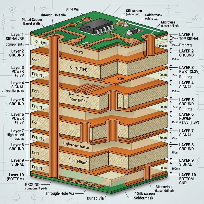
Eine 10-lagige Leiterplatte bietet einen erheblichen Vorteil durch mehrere Routing-Schichten, dedizierte Masseflächen und spezielle Stromversorgungsflächen. Ein typischer 10-lagiger Aufbau könnte wie folgt angeordnet sein: Signal, Masse, Signal, Stromversorgung, Masse, Masse, Stromversorgung, Signal, Masse, Signal. Diese Anordnung wird sehr geschätzt, da sie eine hervorragende Abschirmung für Hochgeschwindigkeits-Signalschichten bietet und sicherstellt, dass sowohl die Stromversorgungs- als auch die Masseebenen eng gekoppelt sind. Diese enge Kopplung reduziert die Impedanz des Stromverteilungsnetzes (PDN), was für die Bewältigung komplexer Stromversorgungsanforderungen in modernen elektronischen Systemen von entscheidender Bedeutung ist.
Indem man Signalschichten zwischen durchgehende Masseflächen einfügt (bekannt als Streifenleitung Konfiguration) können Entwickler die durch Hochfrequenzsignale erzeugten elektromagnetischen Felder wirksam eindämmen. Diese Eindämmung verhindert, dass Energie nach außen abstrahlt und benachbarte Leiterbahnen oder in der Nähe befindliche Bauteile stört. Bei einem 10-lagigen Design haben Sie den Vorteil, mehrere Streifenleitungsschichten einbauen zu können, was die Gesamtleistung drastisch verbessert. Signalintegrität des Systems.
Warum 10 Schichten für das Energiemanagement?
Beim Einsatz von Field-Programmable Gate Arrays (FPGAs), Hochgeschwindigkeitsprozessoren oder hochintegrierten Kommunikationsschnittstellen kann der Strombedarf enorm sein. Diese Bausteine erfordern oft mehrere Spannungsversorgungen – wie beispielsweise 3,3 V, 1,8 V, 1,2 V und sogar Spannungen unter 1 V –, die alle mit minimalem Rauschen und minimalem Spannungsabfall bereitgestellt werden müssen. Die Verwaltung all dieser unterschiedlichen Spannungsversorgungen auf einer Leiterplatte mit geringer Schichtenanzahl zwingt Entwickler dazu, schmale Stromversorgungsbahnen zu verwenden, die naturgemäß eine höhere Induktivität und einen höheren Widerstand aufweisen, was zu einer schlechten Stromversorgung führt.
Bei einem 10-lagigen Leiterplattenaufbau können Ingenieure ganze Lagen bestimmten Versorgungsspannungen zuweisen oder die Ebenen aufteilen, um mehrere Spannungen auf einer einzigen Lage unterzubringen. Durch die Anordnung fester, ununterbrochener Versorgungsebenen neben festen Masseebenen entsteht eine große Eigenkapazität. Diese planare Kapazität wirkt als Hochfrequenz-Entkopplungskondensator, versorgt schnell schaltende ICs sofort mit Strom und reduziert das Rauschen der Stromversorgung erheblich. Ohne diese robuste Stromverteilungsfähigkeit würden Hochgeschwindigkeitssignale unter Jitter leiden, und die Gesamtzuverlässigkeit des Systems würde drastisch sinken.
Wärmemanagement in einem 10-lagigen Schichtaufbau
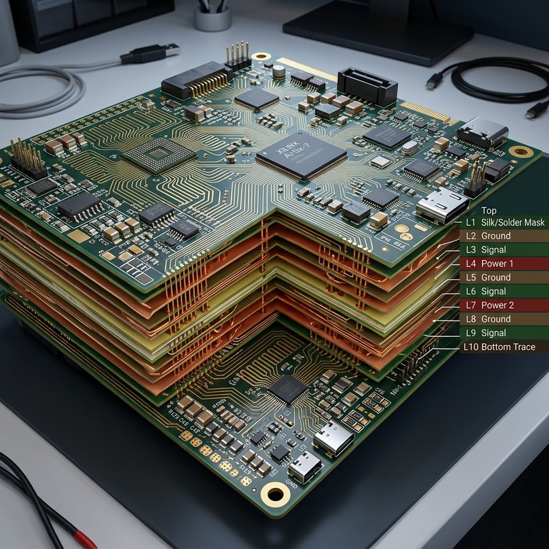
Komplexe Stromversorgungsanforderungen führen unweigerlich zur Wärmeentwicklung. Einer der versteckten Vorteile einer 10-lagigen Leiterplatte ist ihre verbesserte Wärmeableitung. Die großen Mengen an Kupfer in den internen Strom- und Masseebenen wirken als hervorragende Wärmeverteiler. Wenn ein Hochleistungskomponente Wärme erzeugt, kann diese Wärme mithilfe von thermischen Durchkontaktierungen direkt in diese internen Kupferebenen geleitet und über die gesamte Leiterplattenoberfläche verteilt werden, wo sie leichter an die Umgebung abgegeben werden kann.
Da eine 10-lagige Leiterplatte zudem mehr Flexibilität bei der Leiterbahnführung bietet, können Entwickler Hochleistungskomponenten in größerem Abstand zueinander anordnen und so thermische Hotspots vermeiden, die die Zuverlässigkeit des gesamten Systems beeinträchtigen könnten. Ein effektives Wärmemanagement verlängert direkt die Lebensdauer der Komponenten und verhindert katastrophale Ausfälle bei Spitzenauslastungen.
So entwirft man einen robusten 10-lagigen Leiterplattenaufbau
Befolgen Sie diese Schritt-für-Schritt-Anleitung, um einen effektiven 10-lagigen Leiterplattenaufbau zu erstellen, der speziell auf die Bewältigung komplexer Stromversorgungsanforderungen zugeschnitten ist.
Schritt 1: Anforderungen an die Ebenen festlegen
Ermitteln Sie die Gesamtzahl der für die Verdrahtung erforderlichen Signalschichten sowie die Anzahl der Stromversorgungs- und Masseflächen, die zur Versorgung Ihrer Bauteile benötigt werden. Stellen Sie sicher, dass Hochgeschwindigkeitssignale über benachbarte Referenzflächen verfügen.
Schritt 2: Referenzebenen zuweisen
Platzieren Sie massive Masseflächen direkt neben Ihren wichtigsten Hochgeschwindigkeits-Signalschichten. Dadurch wird die Schleifeninduktivität minimiert und das Übersprechen begrenzt. In einem ausgewogenen Schichtaufbau sollten die Masseflächen in der Regel zahlreicher sein als die Versorgungsflächen.
Schritt 3: Stromversorgung und Masse verbinden
Ordnen Sie die Stromversorgungsebenen so nah wie möglich an den Masseebenen an, soweit es die Fertigungstoleranzen zulassen. Dadurch wird die Kapazität zwischen den Ebenen maximiert, was für die Hochfrequenzentkopplung und die Stromversorgungsintegrität von entscheidender Bedeutung ist.
Schritt 4: Den Stapel ausgleichen
Achten Sie darauf, dass der Schichtaufbau symmetrisch um die Mitte der Leiterplatte angeordnet ist. Ein symmetrischer Schichtaufbau verhindert ein Verziehen der Leiterplatte bei den hohen Temperaturen, die während der Fertigungs- und Montageprozesse auftreten.
Schritt 5: Impedanz überprüfen
Verwenden Sie einen Impedanzrechner oder Ihre Leiterplatten-Entwurfssoftware, um zu überprüfen, ob die Leiterbahnbreiten und die Dielektrikumsdicken zu den angestrebten charakteristischen Impedanzen führen (z. B. 50 Ohm Single-Ended, 100 Ohm Differential).
Häufig gestellte Fragen
Was ist der Hauptvorteil einer 10-lagigen Leiterplatte gegenüber einer 8-lagigen Leiterplatte?
Der Hauptvorteil besteht in der Hinzufügung von zwei weiteren Verlegungsschichten bzw. Referenzebenen. Dies ermöglicht eine engere Kopplung zwischen Stromversorgung und Masse, eine bessere Abschirmung für Hochgeschwindigkeitssignale sowie mehr Flexibilität bei der Verlegung für hochdichte Bauteile wie BGAs (Ball Grid Arrays).
Wie dick ist eine handelsübliche 10-lagige Leiterplatte?
Zwar kann dies je nach den spezifischen Konstruktionsanforderungen variieren, doch wird eine standardmäßige 10-lagige Leiterplatte häufig mit einer Gesamtdicke von 0,062 Zoll (1,57 mm) gefertigt. Bei sehr komplexen Schichtaufbauten sind jedoch auch Dicken von 0,093 Zoll oder mehr üblich.
Verbessert eine 10-lagige Leiterplatte die Signalintegrität?
Ja, und zwar erheblich. Durch die Bereitstellung von mehr dedizierten Masseebenen ermöglicht ein 10-lagiger Aufbau die Verlegung von Streifenleitern. Bei Streifenleitern wird die Signalleitung zwischen zwei massiven Masseebenen eingeschlossen, wodurch elektromagnetische Störungen (EMI) und Übersprechen von benachbarten Lagen praktisch ausgeschlossen werden, was die Signalintegrität erheblich verbessert.
Ist die Herstellung einer 10-lagigen Leiterplatte teurer?
Ja, mit steigender Schichtenanzahl nehmen auch die Komplexität der Fertigung und die Materialkosten zu. Der Laminierungsprozess erfordert mehr Zeit und Präzision, um sicherzustellen, dass alle Schichten perfekt aufeinander ausgerichtet sind. Die Kosten werden jedoch oft durch die notwendigen Leistungssteigerungen und die in der High-End-Elektronik geforderte Zuverlässigkeit gerechtfertigt.