In der modernen Hochgeschwindigkeitselektronik ist die 8-lagiger Leiterplattenaufbau hat sich zur Standardwahl für Ingenieure entwickelt, die ein Gleichgewicht zwischen hoher Bauteil-Dichte und hervorragender Signalintegrität, sowie die Kosteneffizienz. Die Entwicklung einer 8-lagigen Leiterplatte erfordert eine sorgfältige Planung und fortschrittliche Verlegungsstrategien, um eine optimale Leistung zu gewährleisten, elektromagnetische Störungen (EMI) zu minimieren und die Stromversorgungsintegrität aufrechtzuerhalten. In diesem umfassenden Leitfaden werden bewährte Verfahren und fortgeschrittene Verlegungstechniken zur Optimierung Ihres 8-lagigen Leiterplatten-Stapelaufbaus vorgestellt.
Das 8-lagige Leiterplatten-Stackup verstehen
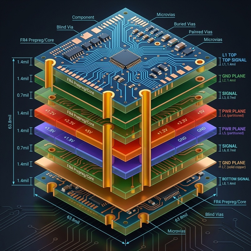
Ein typischer 8-lagiger Leiterplattenaufbau bietet ausreichend Lagen, um kritische Hochgeschwindigkeitssignale von Stromversorgungs- und Masseebenen zu trennen, wodurch Übersprechen und Impedanzfehlanpassungen wirksam reduziert werden. Der Hauptvorteil einer 8-lagigen Konfiguration gegenüber einem 4- oder 6-lagigen Aufbau liegt in der Verfügbarkeit soliderer Masse- und Versorgungsflächen, die bessere Rückleitungswege und eine bessere Abschirmung für empfindliche Leiterbahnen bieten.
Bei der Festlegung Ihres Laminataufbaus ist die Anordnung der Signal-, Stromversorgungs- und Masseebenen von entscheidender Bedeutung. Eine gängige und äußerst effektive Anordnung ist:
- Ebene 1 (oben): Hochgeschwindigkeitssignale, Komponenten
- Ebene 2: Massiv Massefläche
- Ebene 3: Signal (interne Hochgeschwindigkeits-Leitwege)
- Ebene 4: Power Plane
- Schicht 5: Massive Masseplatte
- Schicht 6: Signal (interne Hochgeschwindigkeits-Leitwege)
- Schicht 7: Massive Masseplatte
- Schicht 8 (unten): Signale, Komponenten

Fortgeschrittene Routing-Strategien
Das Verlegen der Leiterbahnen auf einer 8-lagigen Leiterplatte umfasst mehr als nur das Verbinden von Pins. Es erfordert ein tiefgreifendes Verständnis der Theorie der Übertragungsleitungen, Impedanzkontrolle, sowie die Signalintegrität.
1. Impedanzsteuerung und Leiterbahnbreite
Die Aufrechterhaltung einer gleichbleibenden Impedanz über Hochgeschwindigkeits-Leiterbahnen hinweg ist von entscheidender Bedeutung. Jede Abweichung kann zu Signalreflexionen und einer Verschlechterung der Signalqualität führen. Berechnen Sie den erforderlichen Leiterbahnbreite sowie die Abstände entsprechend den Parametern für dielektrische Materialien und Schichtaufbau Ihres Leiterplattenherstellers. Der Einsatz von Differenzpaaren für Hochgeschwindigkeitsschnittstellen wie USB, HDMI und PCIe ist unerlässlich. Stellen Sie sicher, dass die Länge der positiven und negativen Leiterbahnen in einem Differenzpaar exakt aufeinander abgestimmt ist, um Phasenverschiebungen und Gleichtaktstörungen zu vermeiden.
2. Unterdrückung von Übersprechen
Übersprechen tritt auf, wenn das elektromagnetische Feld einer Leiterbahn eine Spannung oder einen Strom in einer benachbarten Leiterbahn induziert. Bei einem 8-lagigen Leiterplattenaufbau können Sie das Übersprechen wie folgt verringern:
- Vergrößerung des Abstands zwischen parallelen Leiterbahnen (gemäß der 3W-Regel, wonach der Abstand das Dreifache der Leiterbahnbreite betragen soll).
- Benachbarte Signalschichten orthogonal (senkrecht) zueinander verlegen, um die parallele Kopplung zu minimieren.
- Effektiver Einsatz von Masseflächen zur Isolierung von Signalschichten.
3. Über das Management
Vias sind für die Signalübertragung zwischen den Schichten erforderlich, führen jedoch zu Impedanzsprüngen. Minimieren Sie die Verwendung von Vias auf kritischen Hochgeschwindigkeits-Leiterbahnen. Wenn sich Vias nicht vermeiden lassen, verwenden Sie in der Nähe liegende Masse-Rückleitungs-Vias, um eine durchgehende Rückweg für die Hochfrequenz-Signalkomponenten. Bei Designs mit extrem hoher Dichte sollten Sie den Einsatz von Blind- oder vergrabenen Durchkontaktierungen in Betracht ziehen, auch wenn dies die Herstellungskosten erhöht.

So entwerfen Sie einen effektiven 8-lagigen Leiterplattenaufbau
Befolgen Sie diese Schritte, um einen robusten und effizienten Aufbau für eine 8-lagige Leiterplatte zu erstellen.
Schritt 1: Signal-Anforderungen definieren
Ermitteln Sie alle Hochgeschwindigkeitssignale, analogen Leiterbahnen und Stromversorgungsanforderungen. Gruppieren Sie zusammengehörige Signale, um die Verlegung und die Zuordnung zu den Schichten zu vereinfachen.
Schritt 2: Masse- und Stromversorgungsebenen zuweisen
Weisen Sie spezielle Schichten für Masseschichten und Stromversorgungsschichten zu. Stellen Sie sicher, dass die Schichten für Hochgeschwindigkeitssignale unmittelbar an eine Masseschicht angrenzen, um einen Rückweg mit niedriger Impedanz zu gewährleisten.
Schritt 3: Festlegung von Routing-Richtlinien
Legen Sie vor Beginn des Routing-Prozesses Designregeln für Leiterbahnbreiten, Abstände, Anforderungen an Differentialpaare und Impedanzziele fest.
Schritt 4: Verlegen Sie kritische Signale zuerst
Legen Sie bei der Leiterbahnführung besonderen Wert auf Hochgeschwindigkeits-Differenzpaare, Taktsignale und empfindliche analoge Signale. Halten Sie diese Leiterbahnen so kurz und direkt wie möglich.
Schritt 5: Durchführung einer Signalintegritätsanalyse
Nutzen Sie Simulationswerkzeuge, um die Impedanzanpassung, die Übersprechwerte und die Stromversorgungsintegrität während der gesamten Entwurfsphase zu überprüfen.
Häufig gestellte Fragen
Warum sollte man sich für einen 8-lagigen Leiterplattenaufbau statt für einen 6-lagigen entscheiden?
Ein 8-lagiger Aufbau bietet zwei zusätzliche Lagen, wodurch stabilere Masseflächen möglich sind. Dies verbessert die elektromagnetische Verträglichkeit (EMV) erheblich, sorgt für eine bessere Abschirmung von Hochgeschwindigkeitssignalen und ermöglicht im Vergleich zu einem 6-lagigen Design sauberere Stromverteilungsnetze.
Wie sieht die optimale Schichtaufbau für eine 8-lagige Leiterplatte aus?
Zwar hängt dies von der jeweiligen Auslegung ab, doch eine gängige optimale Anordnung lautet: Signal 1, Masse, Signal 2, Stromversorgung, Masse, Signal 3, Masse, Signal 4. Dadurch wird sichergestellt, dass jede Hochgeschwindigkeits-Verlegungsschicht über eine angrenzende durchgehende Referenzebene verfügt.
Wie kann ich die Impedanz in meinem 8-lagigen Design steuern?
Die Impedanz wird durch die präzise Berechnung der Leiterbahnbreite, der Leiterbahndicke, der Dielektrizitätskonstante des Leiterplattenmaterials und des Abstands zur benachbarten Referenzebene gesteuert. Die meisten modernen Tools für den Leiterplattenentwurf verfügen über integrierte Impedanzrechner, die bei der Festlegung dieser Parameter helfen.
Schlussfolgerung
Die Beherrschung der 8-lagiger Leiterplattenaufbau ist für die Entwicklung komplexer, leistungsstarker elektronischer Geräte von entscheidender Bedeutung. Durch die Umsetzung dieser fortschrittlichen Verlegungsstrategien, eine sorgfältige Planung Ihres Schichtaufbaus und eine gründliche Prüfung der Signalintegrität können Sie sicherstellen, dass Ihre Entwürfe den hohen Anforderungen moderner Technologie gerecht werden. Arbeiten Sie bereits in einer frühen Phase des Entwurfsprozesses eng mit Ihrem Leiterplattenhersteller zusammen, um die Materialeigenschaften und Fertigungsmöglichkeiten abzustimmen und so eine erfolgreiche Fertigung zu gewährleisten.