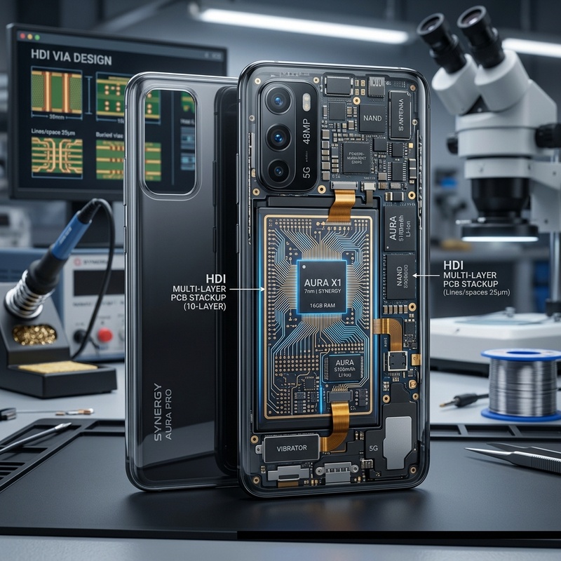
In der sich rasant entwickelnden Welt der Unterhaltungselektronik treibt die Nachfrage nach kleineren, leichteren und leistungsstärkeren Geräten die Innovation weiter voran. Im Zentrum dieser Miniaturisierungsrevolution steht die High-Density-Interconnect-Leiterplatte (HDI-Leiterplatte). Moderne Smart-Geräte – von Smartphones über Wearables bis hin zu fortschrittlichen IoT-Sensoren – sind in hohem Maße auf einen HDI-Leiterplattenaufbau angewiesen, um ihre kompakten Designs zu realisieren, ohne dabei Kompromisse bei Leistung oder Zuverlässigkeit einzugehen. Dieser Artikel befasst sich eingehend mit den Gründen, warum ein HDI-Leiterplattenaufbau für moderne Smart-Geräte unverzichtbar ist, und beleuchtet die zugrunde liegende Technologie, die dies ermöglicht.
Das Streben nach Miniaturisierung
Verbraucher erwarten heute, dass ihre Geräte mehr leisten und dabei weniger Platz beanspruchen. Ein Smartphone ist längst nicht mehr nur ein Kommunikationsmittel, sondern eine hochauflösende Kamera, eine Spielekonsole, ein Fitness-Tracker und ein persönlicher Assistent in einem. Diese immense Funktionalität in einem schlanken, taschengroßen Formfaktor unterzubringen, ist eine gewaltige technische Herausforderung. Herkömmliche Techniken zur Leiterplattenherstellung, die auf standardmäßigen Durchkontaktierungen und breiteren Leiterbahnbreiten basieren, sind für diese Anwendungen mit begrenztem Platzangebot schlichtweg ungeeignet. Hier kommt die HDI-Technologie ins Spiel.
Was ist ein HDI-Leiterplatten-Stackup?
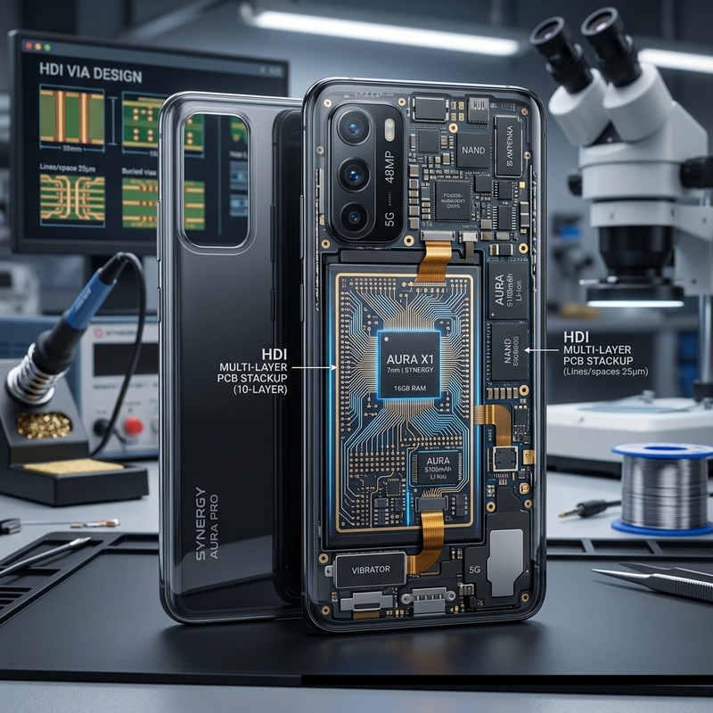
Ein HDI-Leiterplattenaufbau zeichnet sich durch eine höhere Verdrahtungsdichte pro Flächeneinheit im Vergleich zu herkömmlichen Leiterplatten aus. Er nutzt Mikrovias, Blindvias, vergrabene Vias und Aufbauschichten, um Signale effizienter zu leiten. Durch die Minimierung der Größe der Durchkontaktierungen und des Abstands zwischen den Leiterbahnen ermöglicht ein HDI-Leiterplattenaufbau den Entwicklern, mehr Bauteile in engerer Nachbarschaft zueinander zu platzieren. Dies reduziert die Gesamtgrundfläche der Leiterplatte erheblich und ermöglicht die Entwicklung ultrakompakter intelligenter Geräte.
Kernelemente der HDI-Technologie
Der Erfolg eines HDI-Leiterplattenaufbaus hängt von mehreren entscheidenden Konstruktionselementen ab:
- Mikrovias: Es handelt sich hierbei um extrem kleine Durchkontaktierungen mit einem Durchmesser von in der Regel weniger als 150 Mikrometer, die mittels Laserbohrverfahren hergestellt werden. Sie verbinden benachbarte Schichten der Leiterplatte miteinander und sparen so wertvollen Platz auf der Platine.
- Blind- und vergrabene Durchkontaktierungen: Blind-Vias verbinden eine äußere Schicht mit einer oder mehreren inneren Schichten, ohne die gesamte Leiterplatte zu durchdringen. Vergrabene Vias verbinden innere Schichten, ohne die Außenflächen zu erreichen. Beide Techniken schaffen Platz für die Leiterbahnführung auf anderen Schichten.
- Bauteile mit feinem Rasterabstand: HDI-Leiterplatten sind für die Aufnahme von Bauteilen mit sehr engem Pinabstand ausgelegt, wie beispielsweise Ball Grid Arrays (BGAs) und Chip Scale Packages (CSPs).
Vorteile von HDI in intelligenten Geräten
Der Einsatz eines HDI-Leiterplattenaufbaus bietet zahlreiche Vorteile, die sich direkt in besseren Smart-Geräten niederschlagen:
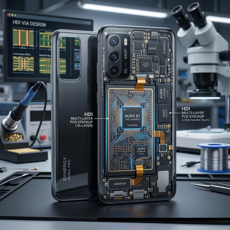
- Geringere Größe und geringeres Gewicht: Durch die Maximierung der Leiterbahndichte reduziert HDI die physische Größe und das Gewicht der Leiterplatte, was für Wearables und tragbare Elektronik von entscheidender Bedeutung ist.
- Verbessert Signalintegrität: Die kürzeren Abstände zwischen den Bauteilen und die geringeren Stichleitungslängen in Mikrovias führen zu einer geringeren Signalverschlechterung, weniger Übersprechen und einer besseren elektrischen Leistung, insbesondere bei hohen Frequenzen.
- Erhöhte Zuverlässigkeit: Die robuste Bauweise der HDI-Mikrovias sorgt für eine hervorragende thermische und mechanische Zuverlässigkeit und gewährleistet, dass Smart-Geräte den Belastungen des täglichen Gebrauchs standhalten können.
- Kosteneffizienz bei komplexen Konstruktionen: Zwar sind die Herstellungskosten pro Quadratzoll einer HDI-Leiterplatte möglicherweise höher, doch durch die Möglichkeit, mehrere Leiterplatten in einer einzigen HDI-Leiterplatte zusammenzufassen, lassen sich die Gesamtsystemkosten senken und die Montage vereinfachen.
So entwirft man einen HDI-Leiterplattenaufbau (Schema.org-Mikrodaten)
Entwurf eines HDI-Leiterplatten-Stapelaufbaus
Ein kurzer Leitfaden zur Gestaltung des Schichtaufbaus einer HDI-Leiterplatte für Smart Devices.
Schritt 1: Anforderungen definieren
Ermitteln Sie die baulichen Einschränkungen, die Anzahl der Schichten und die elektrischen Anforderungen des Smart-Geräts, um die Stapelstruktur zu festzulegen.
Schritt 2: Die richtigen Materialien auswählen
Wählen Sie Kern- und Prepreg-Materialien aus, die die für HDI-Anwendungen erforderlichen Dielektrizitätskonstanten, thermischen Eigenschaften und Maßhaltigkeit aufweisen.
Schritt 3: Planung der Via-Struktur
Platzieren Sie Microvias, Blind-Vias und vergrabene Vias strategisch, um die Verdrahtungsdichte zu optimieren und Signalstörungen.
Schritt 4: Leiterplatte verlegen
Nutzen Sie fortschrittliche CAD-Werkzeuge, um feine Leiterbahnen und Abstände zu verlegen, und stellen Sie dabei sicher, dass die Fertigungsmöglichkeiten und die Richtlinien zur Signalintegrität eingehalten werden.
Schlussfolgerung
Angesichts des anhaltenden Trends zu immer kleineren, schnelleren und leistungsfähigeren Elektronikgeräten kann die Bedeutung des HDI-Leiterplattenaufbaus gar nicht hoch genug eingeschätzt werden. Er ist die grundlegende Schlüsseltechnologie, die es Ingenieuren ermöglicht, hochentwickelte Funktionen in die kompakten Smart-Geräte zu integrieren, auf die wir uns täglich verlassen. Durch die Beherrschung der HDI-Designprinzipien können Hersteller die Grenzen der Innovation weiter verschieben und die nächste Generation revolutionärer Unterhaltungselektronik auf den Markt bringen.
Häufig gestellte Fragen (Schema.org-Mikrodaten)
Wofür steht die Abkürzung HDI in der Leiterplattenfertigung?
HDI steht für „High-Density Interconnect“. Der Begriff bezeichnet eine Technologie zur Herstellung von Leiterplatten, die durch den Einsatz von Mikrovias, feinen Leiterbahnen und dünnen Materialien eine höhere Verdrahtungsdichte pro Flächeneinheit ermöglicht als herkömmliche Leiterplatten.
Warum ist ein HDI-Leiterplattenaufbau für Smartphones unverzichtbar?
Ein HDI-Leiterplattenaufbau ist für Smartphones unverzichtbar, da er die Miniaturisierung der internen Komponenten ermöglicht. Er bietet die erforderliche Verdrahtungsdichte, um moderne Mikroprozessoren, Speicherchips und Sensoren auf dem äußerst begrenzten Raum im Gehäuse eines Smartphones miteinander zu verbinden.
Sind HDI-Leiterplatten in der Herstellung teurer?
Zwar sind die Herstellungskosten pro Quadratzoll einer HDI-Leiterplatte aufgrund fortschrittlicher Verfahren wie Laserbohren und sequenzieller Laminierung in der Regel höher, doch können die Gesamtsystemkosten oft niedriger ausfallen. Dies liegt daran, dass die HDI-Technologie die Gesamtzahl der benötigten Schichten reduzieren, die Leiterplattengröße minimieren und mehrere Leiterplatten zu einer einzigen zusammenfassen kann.