In der modernen Entwurf von Hochgeschwindigkeits-Leiterplatten (PCB), ist die Stromversorgungsintegrität von größter Bedeutung. Eine der grundlegenden Maßnahmen zur Gewährleistung einer stabilen Stromversorgung und zur Unterdrückung hochfrequenter Störsignale ist der effektive Einsatz von Entkopplungskondensatoren. Die richtige Platzierung von Entkopplungskondensatoren auf einer Leiterplatte ist nicht nur eine Empfehlung – sie ist eine entscheidende Voraussetzung für den zuverlässigen Betrieb von Mikrocontrollern, FPGAs und anderen integrierten Schaltkreisen (ICs).
Warum Entkopplungskondensatoren wichtig sind
Wenn ein IC den Zustand wechselt, benötigt er einen plötzlichen Stromstoß. Die Stromversorgung und die zum IC führenden Leiterbahnen weisen eine inhärente Induktivität auf, die dieser schnellen Stromänderung entgegenwirkt. Diese Induktivität verursacht einen lokalen Spannungsabfall (oft als „Ground Bounce“ oder „Voltage Droop“ bezeichnet), der möglicherweise zu Logikfehlern oder System-Resets führen kann. Entkopplungskondensatoren fungieren als lokale Energiespeicher, die dem IC den erforderlichen Momentanstrom liefern und die parasitäre Induktivität des übergeordneten Stromverteilungsnetzes (PDN) umgehen.
Grundprinzipien für die Anordnung von Entkopplungskondensatoren
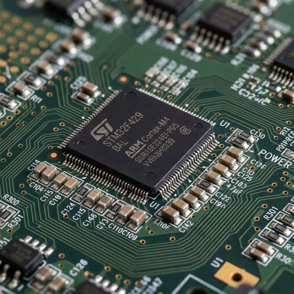
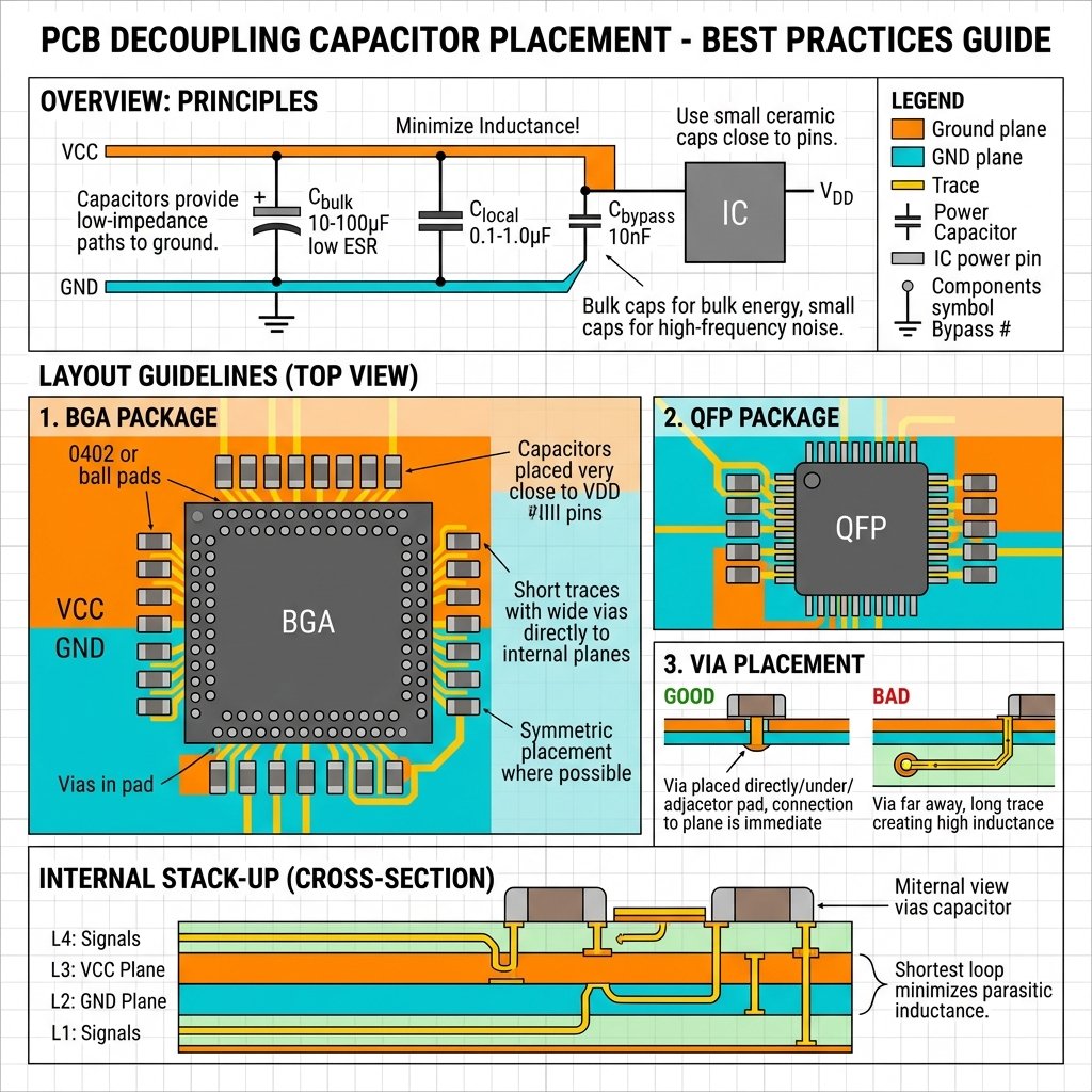
Die goldene Regel der Entkopplung ist einfach: Minimieren Sie die Schleifeninduktivität zwischen dem Kondensator und den IC-Pins, die er entkoppelt. Diese Schleife umfasst den Pfad vom Kondensator zum Stromversorgungs-Pin, durch den IC, hinaus zum Masse-Pin und zurück zum Kondensator. Um diese Schleifenfläche und die damit verbundene Induktivität zu minimieren, befolgen Sie diese wichtigen Richtlinien:
- Nähe ist entscheidend: Platzieren Sie den Entkopplungskondensator so nah wie möglich an den Versorgungs- und Massepins des ICs. Schon wenige zusätzliche Millimeter Leiterbahnlänge können bei hohen Frequenzen eine erhebliche parasitäre Induktivität verursachen, wodurch die Wirksamkeit des Kondensators erheblich beeinträchtigt wird.
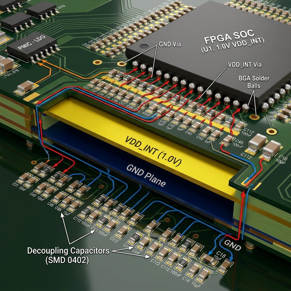
- Anzahl und Länge der Leiterbahnen minimieren: Falls Sie Durchkontaktierungen verwenden müssen, um den Kondensator mit interne Strom- oder Masseflächen, halten Sie diese so kurz wie möglich. Platzieren Sie die Durchkontaktierungen direkt neben den Kondensatorpads. Noch besser ist es, den Kondensator direkt mit den IC-Pins auf derselben Oberflächenlage zu verbinden, sofern das Routing dies zulässt.
- Werte sind wichtig: Verwenden Sie eine Kombination aus verschiedenen Kondensatorwerten. Kondensatoren mit kleineren Nennwerten (z. B. 0,1 µF, 0,01 µF) weisen eine geringere äquivalente Serieninduktivität (ESL) auf und reagieren besser auf hochfrequente Transienten. Größere Kondensatoren (z. B. 10 µF) bewältigen Stromspitzen im niedrigen Frequenzbereich.
Schritt-für-Schritt-Anleitung zur Platzierung von Entkopplungskondensatoren
Befolgen Sie diesen systematischen Ansatz für die optimale Platzierung von Entkopplungskondensatoren auf Leiterplatten, um eine robuste Stromversorgungsintegrität zu gewährleisten.
-
Stromanschlüsse identifizieren:
Ermitteln Sie zunächst alle Pinpaare für Versorgung und Masse auf dem IC, die gemäß dem Datenblatt entkoppelt werden müssen.
-
Kondensatorwerte auswählen:
Wählen Sie geeignete Kondensatorwerte entsprechend dem Frequenzbereich der zu erwartenden Störsignale aus. Eine typische Konfiguration umfasst einen 0,1-µF-Keramikkondensator in der Nähe des Pins und einen 1-µF- oder 10-µF-Großraumkondensator in der Nähe.
-
Setzen Sie den kleinsten Kondensator zuerst ein:
Platzieren Sie den Kondensator mit dem kleinsten Nennwert (niedrigster ESL) so nah wie möglich an den IC-Pins. Dadurch wird sichergestellt, dass Rauschen im höchsten Frequenzbereich sofort gedämpft wird.
-
Anbindungen:
Verlegen Sie kurze, breite Leiterbahnen, die die Kondensatoranschlüsse mit den IC-Pins verbinden. Vermeiden Sie lange, schmale Leiterbahnen, da diese die Induktivität erhöhen.
-
Vias optimal platzieren:
Bei der Verbindung mit internen Ebenen sollten Durchkontaktierungen unmittelbar neben oder sogar innerhalb der Kondensatorpads platziert werden (Via-in-Pad, sofern die Fertigungsmöglichkeiten dies zulassen).
Weiterführende Überlegungen
Bei hochkomplexen Leiterplatten mit dicht bestückten BGA-Gehäusen (Ball Grid Array) ist es unter Umständen nicht möglich, Kondensatoren auf der obersten Schicht neben dem IC zu platzieren. In solchen Fällen sollten die Entkopplungskondensatoren auf der untersten Schicht der Leiterplatte, direkt unter dem IC, platziert werden. Durch diesen Ansatz bleibt die Schleifeninduktivität extrem gering, da die Durchkontaktierungslänge lediglich der Dicke der Leiterplatte entspricht.
Häufig gestellte Fragen
Was passiert, wenn Entkopplungskondensatoren zu weit entfernt angebracht werden?
Befindet sich ein Entkopplungskondensator zu weit vom IC entfernt, wirkt die Verbindungsleitung zwischen beiden als Induktivität. Diese erhöhte Induktivität verhindert, dass der Kondensator bei hochfrequenten Transienten schnell genug Strom liefern kann, wodurch er unwirksam wird und möglicherweise zu Fehlfunktionen des ICs oder zur Abstrahlung elektromagnetischer Störungen (EMI) führt.
Kann ich einen großen Kondensator anstelle mehrerer kleiner verwenden?
Nein, das ist nicht ratsam. Große Kondensatoren (wie Elektrolytkondensatoren oder große Tantalkondensatoren) weisen im Allgemeinen eine höhere äquivalente Serieninduktivität (ESL) auf. Sie können zwar viel Energie speichern, diese jedoch nicht schnell genug entladen, um hochfrequente Schaltstörungen zu bewältigen. Kleine Keramikkondensatoren weisen eine sehr niedrige ESL auf und reagieren schnell auf hochfrequente Transienten. Durch die Verwendung einer Mischung aus verschiedenen Größen lässt sich ein breites Frequenzspektrum abdecken.
Soll der Kondensator zuerst an den IC angeschlossen werden oder an die Durchkontaktierung zur Stromversorgungsebene?
Der Strompfad sollte von der Triebwerksebene, durch die Durchkontaktierung, bis zum Kondensator-Pad, und anschließend an den IC-Pin. Diese Konfiguration stellt sicher, dass der IC seine Energie aus dem lokalen Energiespeicher des Kondensators bezieht und nicht direkt aus der störanfälligeren Versorgungsspannungsfläche.
Schlussfolgerung
Die optimale Platzierung von Entkopplungskondensatoren auf Leiterplatten zu beherrschen, ist eine grundlegende Kompetenz für jeden Hardware-Ingenieur. Indem Sie auf Nähe achten, die Schleifeninduktivität minimieren und die richtige Kombination von Kondensatorwerten wählen, können Sie ein robustes Stromverteilungsnetzwerk sicherstellen. Ein stabiles Stromverteilungsnetzwerk ist das Fundament, auf dem zuverlässige, leistungsstarke Elektronik aufbaut.