Die Welt der Elektronik entwickelt sich rasant weiter, und Hochfrequenzanwendungen sind heute allgegenwärtiger denn je. Das Herzstück dieser modernen Geräte bildet die Hochfrequenz-Leiterplatte (HF-Leiterplatte). Das Design einer HF-Leiterplatte ist eine heikle Kunst und eine strenge Wissenschaft, vor allem weil Hochfrequenzsignale unglaublich anfällig für Signalstörungen, elektromagnetische Störungen (EMI) und Rauschen sind. Dieser umfassende Leitfaden führt Sie durch die wesentlichen Strategien zur Überwindung von Signalstörungen in HF-Leiterplatten-Stapel-Layouts und stellt sicher, dass Ihre Designs selbst in den anspruchsvollsten Umgebungen einwandfrei funktionieren.
RF-Signalstörungen im Leiterplattendesign verstehen
Signalstörungen in einer HF-Leiterplatte können verschiedene Ursachen haben. Übersprechen, elektromagnetische Kopplung, Impedanzfehlanpassungen und eine schlechte Erdung sind einige der Hauptursachen. Im Gegensatz zu digitalen Signalen, die oft ein gewisses Maß an Rauschen tolerieren können, bevor Logikfehler auftreten, verschlechtern sich analoge HF-Signale kontinuierlich, sobald Rauschen auftritt. Diese Verschlechterung führt direkt zu einer geringeren Reichweite, einem niedrigeren Datendurchsatz und einer verminderten Gesamtzuverlässigkeit des Systems.
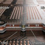
Eine der wirksamsten Methoden zur Behebung dieser Probleme ist ein sorgfältig geplantes PCB-Schichtaufbau. Der Schichtaufbau legt fest, wie Signalschichten, Masseflächen und Stromversorgungsflächen angeordnet sind. Ein gut konzipierter Schichtaufbau bietet dedizierte Rückleitwege, schützt empfindliche Leiterbahnen vor externen Störgrößen und minimiert die Schleifenfläche für hochfrequente Ströme, wodurch die Abstrahlung und die Störanfälligkeit drastisch reduziert werden.
Bei der Auslegung des Schichtaufbaus müssen Ingenieure die dielektrischen Materialien, die Kupferdicke und die genaue Anordnung der Schichten sorgfältig berücksichtigen. Es geht nicht nur darum, Schichten übereinander zu legen, sondern darum, eine dreidimensionale elektromagnetische Umgebung zu schaffen, in der sich HF-Signale ohne Verzerrung oder Dämpfung ausbreiten können.
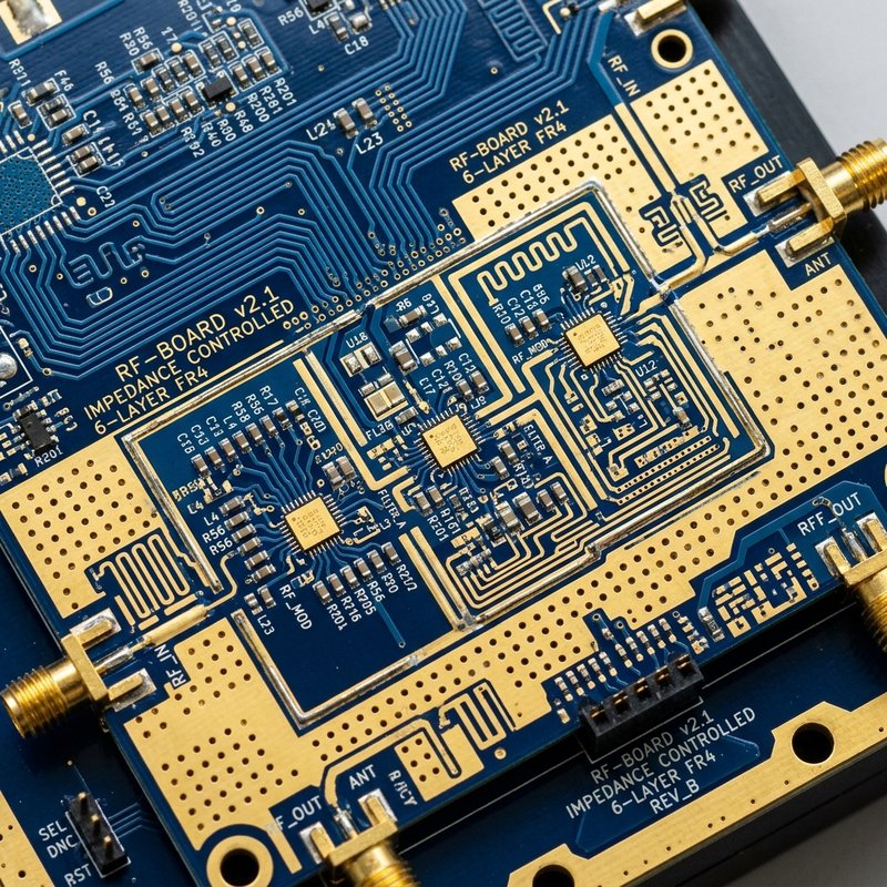
So optimieren Sie das Layout Ihres HF-Leiterplatten-Schichtaufbaus
Die Optimierung des Schichtaufbaus ist ein schrittweiser Prozess, der große Sorgfalt und Liebe zum Detail erfordert. Im Folgenden finden Sie eine umfassende Anleitung, die Ihnen dabei hilft, den Schichtaufbau Ihrer HF-Leiterplatte so zu gestalten, dass Rauschen und Störungen minimiert werden.
Schritt-für-Schritt-Anleitung zur Reduzierung von Störungen in HF-Leiterplatten
Ein ausführlicher, praxisorientierter Leitfaden zur Organisation und Optimierung Ihres HF-Leiterplatten-Laminats, um Rauschen, Übersprechen und Signalstörungen wirksam zu minimieren.
1. Wählen Sie die richtigen dielektrischen Werkstoffe aus
Die Grundlage jeder HF-Leiterplatte ist ihr Substrat. Standard-FR4-Material ist für Hochfrequenz-Anwendungen oft unzureichend, da es einen relativ hohen Verlustfaktor (Df) und eine bei hohen Frequenzen schwankende Dielektrizitätskonstante (Dk) aufweist. Um Signalverluste zu vermeiden und eine konstante Impedanz zu gewährleisten, sollten Sie sich für fortschrittliche Hochfrequenzmaterialien wie PTFE (Teflon), Rogers-Laminate oder keramikgefüllte Kohlenwasserstoffmaterialien entscheiden. Diese Substrate bieten die für HF-Signale erforderliche thermische und elektrische Stabilität.
2. Anordnung und Trennung der Schichten optimieren
Bei einer Mixed-Signal-Leiterplatte ist es von entscheidender Bedeutung, HF-Signale von digitalen und analogen Niederfrequenzsignalen zu trennen. Verwenden Sie einen mehrschichtigen Schichtaufbau, um diese verschiedenen Bereiche voneinander zu isolieren. Die wichtigste Regel lautet, die HF-Signalschicht unmittelbar neben einer massiven, durchgehenden Grundplatte. Diese Nähe gewährleistet eine enge Kopplung und eine niedrige Impedanz Rückweg für die Hochfrequenzströme, wodurch die Schleifeninduktivität und die abgestrahlten Störungen drastisch minimiert werden.
3. Strenge Erdungstechniken anwenden
Die Erdung ist wohl der wichtigste Aspekt beim Entwurf von HF-Leiterplatten. Eine solide, durchgehende Erdungsfläche ist unverzichtbar. Teilen Sie die Erdungsfläche unter HF-Bauteilen oder Leiterbahnen nicht auf, da dies den Rückstrom dazu zwingt, einen längeren Weg mit höherer Impedanz zu nehmen, wodurch eine größere Schleifenfläche entsteht, die Energie abstrahlt. Verwenden Sie außerdem reichlich Masse-Vias – oft als „Via-Stitching“ bezeichnet –, um Masseebenen über mehrere Schichten hinweg zu verbinden. Dies unterdrückt parasitäre Resonanzen und isoliert HF-Abschnitte voneinander.
4. Leitungsführung und kontrollierte Impedanz verwalten
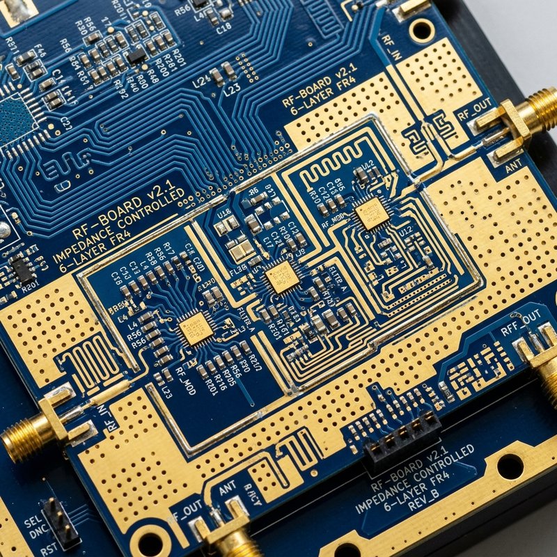
Um Signalreflexionen zu vermeiden, die zu stehenden Wellen und Störungen führen, muss die Impedanz aller HF-Leiterbahnen streng kontrolliert werden, in der Regel auf 50 Ohm. Halten Sie HF-Leiterbahnen so kurz und gerade wie möglich. Vermeiden Sie scharfe 90-Grad-Ecken, da diese Schwankungen in Leiterbahnbreite sowie Impedanzsprünge; verwenden Sie stattdessen gekrümmte Leiterbahnen oder 45-Grad-Winkel. Stellen Sie sicher, dass die Leiterbahnbreite und der dielektrische Abstand über den gesamten Verlegungsverlauf hinweg konstant bleiben.
5. Einsatz von Abschirmungen und Trennzäunen
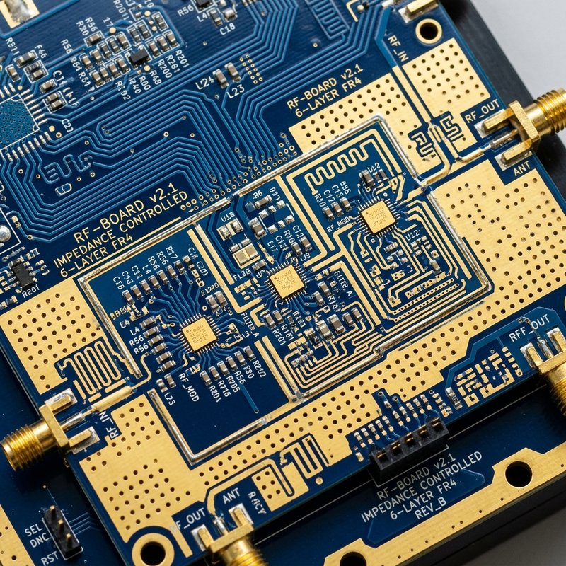
Bei hochempfindlichen HF-Schaltungen sollten Sie den Einsatz einer physikalischen Abschirmung auf Leiterplattenebene in Betracht ziehen. Über HF-Transceivern oder Verstärkern können Abschirmgehäuse angebracht werden, um externe elektromagnetische Störungen (EMI) abzublocken. Innerhalb der Leiterplatte selbst können Sie Via-Zäune anlegen – eine Reihe eng beieinanderliegender Masse-Vias entlang einer HF-Leiterbahn –, um eine lokale, koaxialähnliche Abschirmung zu schaffen. Dies verhindert Übersprechen zwischen parallelen Leiterbahnen und isoliert das HF-Signal vom Rest der Elektronik der Leiterplatte.
Häufig gestellte Fragen (FAQ)
Was ist die häufigste Ursache für Signalstörungen bei HF-Leiterplatten?
Die häufigste Ursache für Signalstörungen bei HF-Leiterplatten ist eine unzureichende Erdung in Verbindung mit einem schlecht geplanten Schichtaufbau. Wenn Erdungsflächen fragmentiert sind oder HF-Leiterbahnen ohne zusammenhängende, angrenzende Erdungsreferenz verlegt werden, führen die daraus resultierenden elektromagnetischen Störungen (EMI) und Übersprechen zu einer erheblichen Verschlechterung Signalintegrität.
Kann ich für HF-Leiterplatten-Schichtaufbauten handelsübliches FR4-Material verwenden?
Standard-FR4 kann für HF-Anwendungen im niedrigen Frequenzbereich verwendet werden, in der Regel für solche unterhalb von 1 GHz. Mit steigender Frequenz werden jedoch der höhere dielektrische Verlust und die instabile Dielektrizitätskonstante von FR4 zum Problem. Für Hochfrequenz-Designs werden spezielle Materialien mit niedrigen Verlustwinkeln dringend empfohlen.
Warum ist eine kontrollierte Impedanz beim HF-Design so entscheidend?
Kontrollierte Impedanz ist von entscheidender Bedeutung, da sich HF-Signale wie Wellen verhalten. Wenn die Impedanz entlang der Übertragungsleitung schwankt, wird ein Teil des Signals zurück zur Quelle reflektiert. Diese Reflexionen verursachen Leistungsverluste, erzeugen stehende Wellen und verzerren das Signal, was zu einer erheblichen Leistungsminderung führt.
Inwiefern verbessern Via-Fences die HF-Leistung von Leiterplatten?
Via-Zäune bestehen aus Reihen geerdeter Vias, die entlang der HF-Leiterbahnen angeordnet sind. Sie wirken wie ein Faraday-Käfig innerhalb des Leiterplattensubstrats, verhindern, dass elektromagnetische Felder aus dem Leiterbahnbereich entweichen, und verhindern, dass externes Rauschen in das empfindliche HF-Signal eingekoppelt wird, wodurch das Übersprechen erheblich reduziert wird.
Schlussfolgerung
Die Beherrschung der Komplexität von HF-Leiterplatten-Stackup-Layouts ist unerlässlich, um Signalstörungen zu überwinden und eine optimale Geräteleistung zu gewährleisten. Durch die sorgfältige Auswahl der richtigen hochfrequenten dielektrischen Materialien, die gewissenhafte Planung Ihrer Schichtaufbau, die strenge Kontrolle der Leiterbahnimpedanz sowie den Einsatz robuster Erdungs- und Abschirmtechniken können Sie Rauschen und elektromagnetische Störungen erfolgreich mindern. Denken Sie daran: Jede Leiterbahn, jede Durchkontaktierung und jede Ebene in einem HF-Design wirkt wie eine potenzielle Antenne oder ein potenzieller Empfänger; die Betrachtung des gesamten Schichtaufbaus als ein zusammenhängendes, fein abgestimmtes elektromagnetisches Umfeld ist der Schlüssel zur Erzielung einer beispiellosen Signalintegrität.