Einführung in den Aufbau von Hochgeschwindigkeits-Leiterplatten
In der modernen Elektronik hat der Bedarf an schnelleren Datenübertragungsraten und höheren Verarbeitungsgeschwindigkeiten zu einer erheblichen Zunahme der Komplexität bei der Entwicklung von Leiterplatten (PCB) geführt. Das Herzstück eines zuverlässigen Hochgeschwindigkeitsdesigns ist die Hochgeschwindigkeits-Leiterplattenaufbau. Bei einem richtig konfigurierten Schichtaufbau geht es nicht nur um die Anordnung der Schichten; er bildet die Grundlage dafür, dass Signalintegrität, die Minimierung elektromagnetischer Störungen (EMI) und die Aufrechterhaltung der Stabilität des Stromversorgungsnetzes (PDN). Das Verständnis der grundlegenden Regeln für den Aufbau von Hochgeschwindigkeits-Leiterplatten ist für Hardware-Ingenieure und Leiterplattenentwickler von entscheidender Bedeutung, die ihre Entwürfe bereits beim ersten Durchlauf erfolgreich umsetzen möchten.
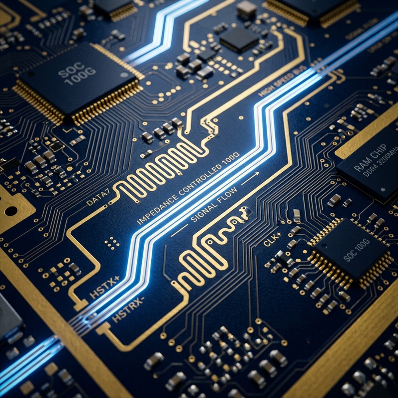
Wenn Signale von niedrigen auf hohe Frequenzen übergehen (typischerweise über 50 MHz oder mit Anstiegszeiten von weniger als 1 ns), können die Leiterbahnen auf der Leiterplatte nicht mehr als einfache Drähte betrachtet werden. Sie werden zu Übertragungsleitungen, bei denen Impedanz, Reflexion und Übersprechen eine wesentliche Rolle spielen. Ein gut durchdachter Schichtaufbau trägt dazu bei, diese Übertragungsleitungseffekte zu kontrollieren, indem geeignete Referenzebenen bereitgestellt, die Dielektrikumsdicke gesteuert und die Schichtzuordnung optimiert werden.
In diesem umfassenden Leitfaden werden wir uns eingehend mit den wichtigsten Regeln und bewährten Verfahren für die Konfiguration eines Hochgeschwindigkeits-Leiterplattenaufbaus befassen. Wir werden dabei unter anderem auf die Anordnung der Schichten eingehen, Impedanzkontrolle, Materialauswahl und bieten eine Schritt-für-Schritt-Anleitung, die Ihnen dabei hilft, einen optimalen Laminataufbau für Ihr nächstes Hochgeschwindigkeitsprojekt zu erstellen.
Grundprinzipien des Aufbaus von Hochgeschwindigkeits-Leiterplatten
Bei der Auslegung eines Hochgeschwindigkeits-Leiterplattenaufbaus muss ein ausgewogenes Verhältnis zwischen elektrischer Leistung, Herstellbarkeit und Kosten gefunden werden. Hier sind die wichtigsten Grundsätze, die es zu beachten gilt:
- Signalschichten, die an massive Ebenen angrenzen: Hochgeschwindigkeitssignale sollten stets auf Schichten verlegt werden, die an eine durchgehende Referenzebene (entweder Masse oder Stromversorgung) angrenzen. Dadurch wird die Schleifenfläche für Rückströme minimiert, was wiederum die elektromagnetische Störung (EMI) und das Übersprechen reduziert.
- Enge Kopplung von Stromversorgung und Masse: Wenn man Strom- und Masseflächen nahe beieinander anordnet (mit einem dünnen Dielektrikum), erhöht sich die Kapazität zwischen den Ebenen. Dies sorgt für eine hervorragende Hochfrequenz-Entkopplung und senkt die Impedanz des PDN bei hohen Frequenzen.
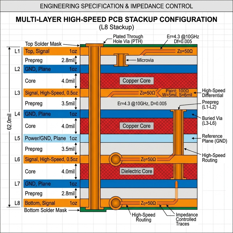
- Symmetrischer Aufbau: Ein Schichtaufbau sollte um die Mitte der Leiterplatte symmetrisch sein, um ein Verziehen während des Herstellungsprozesses zu verhindern. Dies gilt für die Kupferdicke, die Dielektrikumsdicke sowie die Anordnung der Grund- und Signalschichten.
- Vermeiden Sie die Verlegung auf benachbarten Signalschichten: Wenn zwei Signalschichten nebeneinander liegen müssen, sollte die Verlegung streng orthogonal (senkrecht) erfolgen, um das seitliche Übersprechen zu minimieren. Im Allgemeinen ist es jedoch besser, die Signalschichten durch eine Referenzebene voneinander zu trennen.
So konfigurieren Sie einen Leiterplattenaufbau für Hochgeschwindigkeitsanwendungen
Befolgen Sie diese Schritt-für-Schritt-Anleitung, um eine optimierte Hochgeschwindigkeits-Leiterplatten-Schichtkonfiguration zu erstellen, die die Signalintegrität gewährleistet und elektromagnetische Störungen (EMI) minimiert.
Schritt 1: Bestimmen Sie die Anzahl der Schichten
Beginnen Sie mit einer Analyse der Komplexität Ihrer Schaltung. Berechnen Sie die Gesamtzahl der benötigten Signalnetze und konzentrieren Sie sich dabei insbesondere auf Hochgeschwindigkeitsschnittstellen wie PCIe, DDR oder USB. Schätzen Sie die Routing-Dichte ein, um festzustellen, ob Sie 4, 6, 8 oder mehr Schichten benötigen. Sehen Sie stets genügend Schichten für dedizierte Masse- und Versorgungsflächen vor.
Schritt 2: Referenzebenen zuweisen
Ordnen Sie Masse- und Stromversorgungsebenen strategisch zu. Masseebenen werden im Allgemeinen als Referenzebenen für Hochgeschwindigkeitssignale bevorzugt, da sie eine geringere Impedanz aufweisen. Stellen Sie sicher, dass jede Hochgeschwindigkeitssignalebene an mindestens eine durchgehende Masseebene angrenzt. Grundplatte. Bei Leiterplatten mit hoher Schichtenanzahl sollten Signal- und Flächenlagen abwechselnd angeordnet werden.
Schritt 3: Auswahl der richtigen dielektrischen Materialien
Standard-FR4 ist aufgrund hoher dielektrischer Verluste (Verlustfaktor, Df) und einer ungleichmäßigen Dielektrizitätskonstante (Dk) möglicherweise nicht für sehr schnelle Schaltungen geeignet. Wählen Sie je nach Ihren Frequenzanforderungen verlustarme Materialien wie Megtron 6, Rogers oder Isola. Achten Sie auf die Art des Glasfasergewebes, um Auswirkungen des Gewebes auf Differenzpaare zu vermeiden.
Schritt 4: Berechnung und Festlegung der kontrollierten Impedanz
Verwenden Sie einen Impedanzrechner oder den Stackup-Manager Ihres EDA-Tools, um die Leiterbahnbreiten und Abstände festzulegen, die erforderlich sind, um Ihre Zielimpedanz zu erreichen (z. B. 50 Ohm Single-Ended, 100 Ohm Differential). Passen Sie die Dielektrikumsdicke und die Kupferdicke in Ihrem Stackup an, bis die Impedanzziele erreicht sind.
Schritt 5: Überprüfung der Symmetrien und der Herstellbarkeit
Überprüfen Sie den endgültigen Schichtaufbau, um sicherzustellen, dass er von oben bis unten symmetrisch ist. Ziehen Sie Ihren Leiterplattenhersteller frühzeitig in den Prozess ein. Stellen Sie ihm Ihren vorgeschlagenen Schichtaufbau und Ihre Impedanzanforderungen zur Verfügung, damit er diese anhand seiner Fertigungskapazitäten überprüfen und gegebenenfalls Anpassungen vorschlagen kann, die sich aus seinem spezifischen Materialbestand ergeben.
Weiterführende Überlegungen
Über die Grundlagen hinaus umfasst der Aufbau von Hochgeschwindigkeits-Leiterplatten fortgeschrittene Techniken wie die Verwaltung von Durchkontaktierungen und den Einsatz von Mikrovias (HDI). Wenn ein Hochgeschwindigkeitssignal zwischen den Schichten wechselt, muss auch der Rückstrom die Referenzebenen wechseln. Die Platzierung einer Verbindungsvia (die die beiden Masseebenen verbindet) in der Nähe der Signalvia bietet einen niederohmigen Pfad für den Rückstrom, wodurch Emissionen verhindert und die Signalintegrität gewahrt werden.
Die HDI-Technologie (High-Density Interconnect), bei der Blind- und Buried-Vias zum Einsatz kommen, ermöglicht eine kompaktere Leiterbahnführung und weniger Schichtwechsel. HDI-Schichtaufbauten können die Hochgeschwindigkeitsleistung erheblich verbessern, indem sie Via-Stubs reduzieren, die als Antennen wirken und bei hohen Frequenzen Reflexionen verursachen.
Häufig gestellte Fragen (FAQ)
Warum wird Standard-FR4 nicht immer für den Aufbau von Hochgeschwindigkeits-Leiterplatten empfohlen?
Standard-FR4 weist einen relativ hohen Verlustfaktor (Df) auf, was bedeutet, dass es bei hohen Frequenzen mehr Signalenergie absorbiert, was zu einer Signaldämpfung führt. Zudem kann seine Dielektrizitätskonstante (Dk) aufgrund der Glasfasergewebe-Struktur über die Leiterplatte hinweg variieren, was zu einer Verzögerung bei Differentialpaaren führt. Für Hochgeschwindigkeitsanwendungen werden verlustarme Materialien mit stabiler Dk bevorzugt.
Wie wirkt sich die Schichtaufbauweise auf elektromagnetische Störungen (EMI) aus?
Der Schichtaufbau wirkt sich direkt auf die Schleifenfläche der Rückströme aus. Bei einem gut konzipierten Schichtaufbau werden die Signalschichten direkt neben massiven Referenzebenen angeordnet. Dadurch wird das Signal eng mit seiner Rückweg, wodurch die Schleifenfläche minimiert wird. Eine kleinere Schleifenfläche strahlt weniger elektromagnetische Energie ab, wodurch die elektromagnetischen Störungen deutlich reduziert werden.
Wie viele Schichten sollte eine Hochgeschwindigkeits-Leiterplatte idealerweise haben?
Es gibt keine einheitliche “ideale” Schichtenanzahl, da diese von der Komplexität der Schaltung, der Verdrahtungsdichte und der Anzahl der Hochgeschwindigkeitsschnittstellen abhängt. Für robuste Hochgeschwindigkeitsdesigns gelten jedoch häufig 6 bis 8 Schichten als Ausgangspunkt, um ausreichend Platz für die Verdrahtung zu gewährleisten und gleichzeitig geeignete Referenzebenen für alle kritischen Signale beizubehalten.
Schlussfolgerung
Die Konfiguration eines Hochgeschwindigkeits-Leiterplattenaufbaus ist eine komplexe, aber unverzichtbare Aufgabe, die die Gesamtleistung und Zuverlässigkeit des elektronischen Systems maßgeblich bestimmt. Durch die Einhaltung grundlegender Regeln – wie die Gewährleistung benachbarter Referenzebenen, die Wahrung der Symmetrie des Schichtaufbaus, die Auswahl geeigneter Materialien und die sorgfältige Steuerung der Impedanz – können Entwickler häufige Hochgeschwindigkeitsprobleme wie Übersprechen, Reflexionen und EMI mindern. Arbeiten Sie stets eng mit Ihrem Leiterplattenhersteller zusammen, um sicherzustellen, dass Ihr Schichtaufbau sowohl elektrisch einwandfrei als auch gut herstellbar ist. Eine solide Grundlage für den Schichtaufbau ist der erste Schritt zu einem erfolgreichen Hochgeschwindigkeits-Leiterplattendesign.