When designing a Printed Circuit Board (PCB), one of the most critical considerations is the sizing of holes for through-hole components. The PCB hole size you choose directly impacts the ease of assembly, the reliability of the solder joints, and the overall mechanical stability of the final product. Choosing a hole that is too small can make it impossible to insert components, while a hole that is too large can lead to weak solder joints, poor electrical connectivity, and component misalignment. In this comprehensive guide, we will delve deeply into the intricacies of selecting the optimal PCB hole size for your through-hole components to ensure a flawless manufacturing process.
Understanding Through-Hole Technology
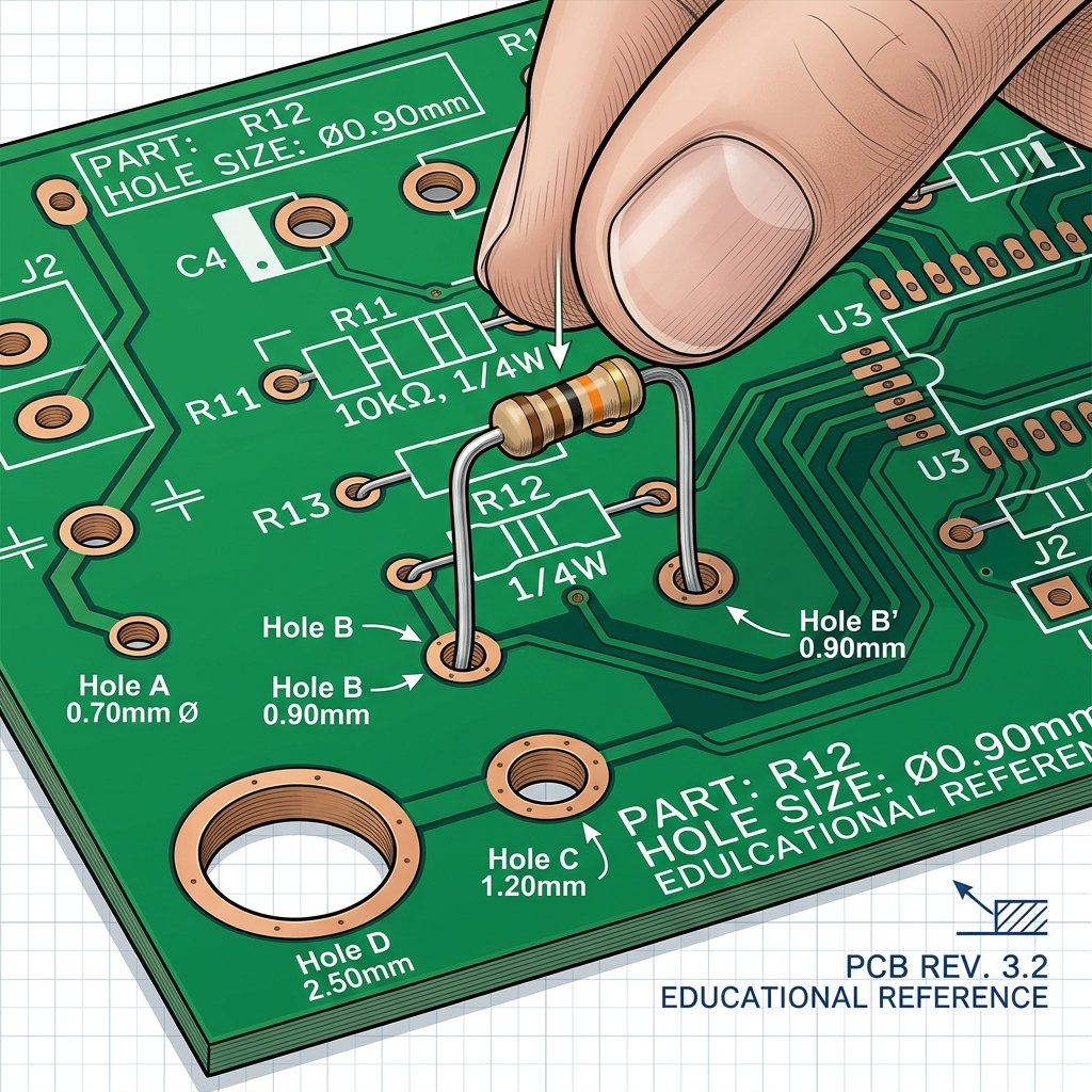
Through-hole technology (THT) involves drilling holes through a printed circuit board and inserting the leads of components such as resistors, capacitors, and integrated circuits through these holes. These leads are then soldered to pads on the opposite side of the board. Despite the widespread adoption of Surface Mount Technology (SMT), through-hole components remain essential for applications requiring strong mechanical bonds, high power handling capabilities, or when specific components are only available in through-hole packages. The integrity of these connections hinges significantly on the precise calculation and specification of the PCB hole size.
Key Factors Influencing PCB Hole Size Selection
Several critical factors must be taken into account when determining the appropriate PCB hole size for a given component:
- Component Lead Diameter or Shape: The primary driving factor is the physical dimension of the component’s lead. Leads can be round, square, or rectangular. The hole must be large enough to accommodate the maximum tolerance of the lead.
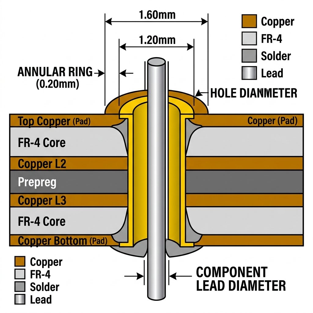
- Plating Thickness: For Plated Through-Holes (PTH), the manufacturer will apply a layer of copper (and usually a surface finish) to the inside walls of the drilled hole. This plating reduces the effective diameter of the hole. Therefore, the drill size must be larger than the final finished hole size required by the component.
- Manufacturing Tolerances: PCB manufacturers have specific tolerances for both the drilling process and the plating process. These tolerances must be factored into your calculations to guarantee the component will always fit, even in the worst-case scenario.
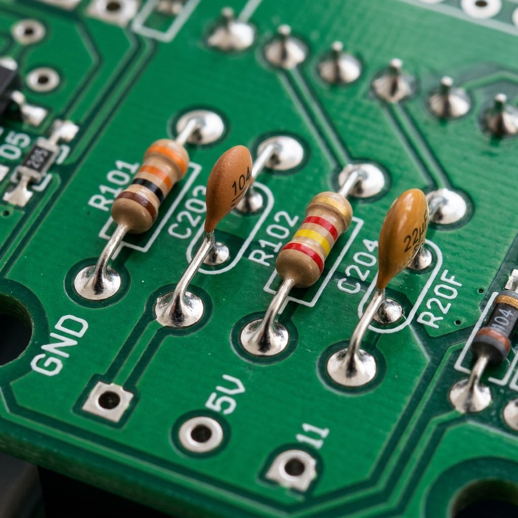
- Soldering Process: Automated soldering processes like wave soldering require adequate capillary action for the molten solder to flow up through the hole and form a strong fillet. A hole that is too tight can restrict this flow, while a hole that is too loose might allow the solder to drain out before solidifying.
How to Calculate the Correct PCB Hole Size
Calculating the right PCB hole size requires a systematic approach to ensure optimal fit and solderability. Follow these steps to determine the correct dimensions.
Step 1: Determine the Maximum Lead Dimension
Step 2: Add the Minimum Clearance
Step 3: Account for Plating Thickness (for Drill Size)
Step 4: Verify Annular Ring Requirements
The Importance of the Annular Ring
Die annular ring is the area of the copper pad that surrounds the drilled and plated hole. A robust annular ring is crucial for the structural integrity of the pad and for ensuring a reliable connection between the component lead and the PCB traces. If the drill wanders slightly during manufacturing (drill registration error), a too-small annular ring can result in a breakout, where the hole breaches the edge of the pad. This can cause open circuits or unreliable connections. Always consult your PCB manufacturer’s capabilities to determine the minimum acceptable annular ring size and design your pads accordingly.
Häufig gestellte Fragen
What happens if a PCB hole size is too small?
What happens if a PCB hole size is too large?
What is the difference between NPTH and PTH?
Schlussfolgerung
Mastering the art of selecting the correct PCB hole size is a fundamental skill for any hardware designer. By meticulously reviewing component datasheets, understanding manufacturing tolerances, and following industry best practices for clearances and annular rings, you can ensure that your through-hole components assemble smoothly and perform reliably for the lifetime of the product. Taking the time to calculate these dimensions accurately during the design phase will save you immense time, cost, and frustration during manufacturing and testing.