When it comes to manufacturing electronic devices, the foundation of a reliable printed circuit board (PCB) lies in its design, particularly the pad layout. Surface Mount Technology (SMT) has become the industry standard for PCB assembly, but its success heavily relies on proper PCB pad design. A poorly designed pad can lead to a host of manufacturing defects, including tombstoning, solder bridging, and weak solder joints, all of which compromise the functionality and longevity of the final product. In this comprehensive guide, we will explore essential PCB pad design tips that will help you achieve reliable SMT assembly and eliminate common soldering defects.

The Importance of Pad Design in SMT Assembly
The PCB pad is the physical interface between the electronic component and the circuit board. It provides the mechanical support to hold the component in place and the electrical connection to the rest of the circuit. In SMT assembly, solder paste is applied to these pads, components are placed on top, and the entire board is heated in a reflow oven to melt the solder and form a strong bond. If the pad dimensions are incorrect, the surface tension of the molten solder can pull the component out of alignment or cause other defects.
Types of PCB Pads
There are generally two types of pads used in SMT design: Non-Solder Mask Defined (NSMD) and Solder Mask Defined (SMD) pads.
- Non-Solder Mask Defined (NSMD): Also known as copper-defined pads, these have a solder mask opening that is larger than the copper pad. This allows the solder to bond to both the top and the sides of the copper pad, providing a stronger mechanical bond. NSMD pads are generally preferred for most SMT components, especially Ball Grid Arrays (BGAs).
- Solder Mask Defined (SMD): For SMD pads, the solder mask overlaps the edge of the copper pad. The size of the exposed pad is defined by the solder mask opening. While this can help prevent pad lifting, it reduces the surface area available for soldering and can lead to stress concentration.
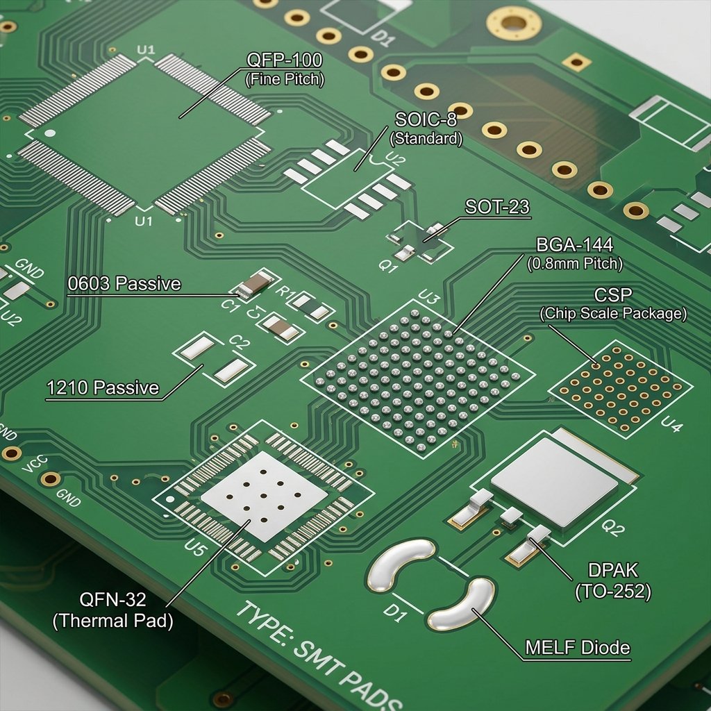
How to Design Perfect PCB Pads for SMT
Follow these steps to ensure your PCB pads are optimally designed for Surface Mount Technology assembly.
Step 1: Consult Component Datasheets
The first and most crucial step in pad design is to refer to the manufacturer’s datasheet for the specific component you are using. The datasheet will almost always provide a recommended land pattern or footprint. These recommendations are based on extensive testing and are designed to yield the best soldering results. Always prioritize the manufacturer’s guidelines over generic calculators.
Step 2: Understand IPC Standards
Familiarize yourself with the IPC-7351 standard, which provides generic requirements for surface mount design and land pattern standards. IPC-7351 defines three density levels for pad geometries: Level A (Maximum Land Protrusion), Level B (Median Land Protrusion), and Level C (Minimum Land Protrusion). For most standard applications, Level B is recommended as it provides a good balance between robust solder joints and space conservation.
Step 3: Calculate the Right Aspect Ratio
The aspect ratio of the pad must match the component lead. If a pad is too long, it can lead to excess solder accumulation. If it’s too wide, it increases the risk of solder bridging between adjacent pads, especially for fine-pitch components. Ensure the pad width is slightly larger than the component lead width to allow for a good solder fillet.
Step 4: Manage Solder Paste Volume
The design of the pad directly affects the amount of solder paste applied during the stencil printing process. Work with your assembly house to design a paste stencil that delivers the correct volume of solder. Too much paste causes bridging; too little causes weak joints. Often, the stencil aperture is slightly smaller than the pad size to prevent excess solder.
Step 5: Account for Thermal Relief
When connecting an SMT pad to a large copper plane (like a Grundplatte), always use Wärmeentlastung connections. A solid connection will act as a heat sink during the reflow process, drawing heat away from the pad and potentially causing a cold solder joint or tombstoning. Thermal reliefs restrict heat flow, ensuring the pad reaches the correct soldering temperature.

Avoiding Common Pad Design Mistakes
To ensure a smooth manufacturing process, avoid these common pitfalls:
- Asymmetrical Pads for 2-Pin Components: For components like chip resistors and capacitors, the pads on both sides must be identical in size and connected to traces of similar width. Asymmetry causes uneven heating during reflow, leading to the “tombstone” effect where the component stands on one end.
- Vias in Pads: Placing a via directly inside an SMT pad (unless it’s a plugged and plated-over via) is a recipe for disaster. During reflow, the solder will wick down the via hole, leaving insufficient solder on the pad to secure the component. If you must place a via near a pad, ensure there is an adequate solder mask dam between them.
- Ignoring Clearances: Ensure there is enough clearance between pads to prevent solder bridging. This is especially critical for fine-pitch ICs (Integrated Circuits) where pads are very close together.
Häufig gestellte Fragen
What is the difference between an NSMD and SMD pad?
An NSMD (Non-Solder Mask Defined) pad has a solder mask opening larger than the copper pad, allowing solder to bond to the top and sides of the pad. An SMD (Solder Mask Defined) pad has the solder mask overlapping the copper, defining the exposed area. NSMD generally provides a stronger solder joint and is preferred for most applications.
What causes tombstoning in SMT assembly?
Tombstoning is typically caused by uneven heating or unequal surface tension forces on the two ends of a passive component during reflow soldering. This can be caused by asymmetrical pad sizes, traces of different widths connecting to the pads, or uneven solder paste application.
Can I place a via in a surface mount pad?
Generally, no. Standard vias in pads will cause the solder to wick away from the pad down into the hole, resulting in a weak or open connection. The exception is if you use a specific manufacturing process called “via-in-pad plated over” (VIPPO), where the via is filled with epoxy and plated over with copper to create a flat, solid pad.
Schlussfolgerung
Proper PCB pad design is not just a matter of following software defaults; it requires a deep understanding of the manufacturing process, component specifications, and industry standards like IPC-7351. By paying close attention to pad dimensions, thermal reliefs, and avoiding common mistakes like vias-in-pad, you can significantly improve the yield and reliability of your SMT assemblies. Always work closely with your PCB fabrication and assembly partners, as their capabilities and processes can also influence your optimal design choices.