Bei der Entwicklung von Leiterplatten (PCBs) für die Leistungselektronik, Motorantriebe oder Hochleistungs-LED-Arrays ist der sichere Umgang mit hohen Strömen eine der größten Herausforderungen. Im Gegensatz zu digitalen Logikplatinen, bei denen Signalintegrität Da dies das Hauptanliegen ist, müssen Hochstrom-Leiterplatten erhebliche Leistungen bewältigen, ohne auszufallen, in Brand zu geraten oder die Lebensdauer der Leiterplatte zu beeinträchtigen. Der wichtigste Mechanismus hierfür ist die Bestimmung der richtigen Leiterbahnbreite.
In diesem umfassenden Leitfaden befassen wir uns mit den physikalischen und mathematischen Grundlagen zur Berechnung der idealen Leiterbahnbreite für Hochstromanwendungen, den für diese Berechnungen geltenden Normen sowie praktischen Tipps, um die Sicherheit und Zuverlässigkeit Ihrer Entwürfe zu gewährleisten.
Die Physik von Leiterbahnmustern und Strom auf Leiterplatten
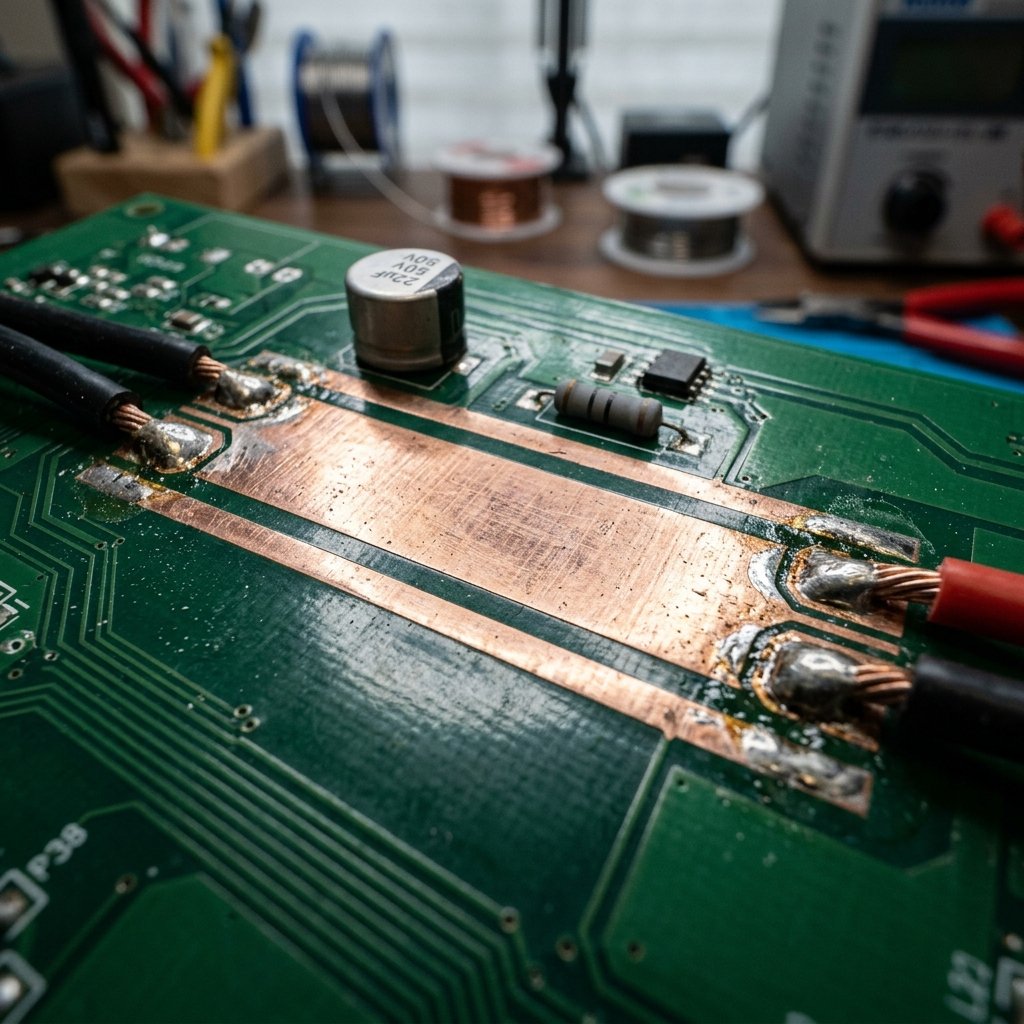
Eine Leiterbahn auf einer Leiterplatte ist im Wesentlichen ein flacher, rechteckiger Draht. Wie jeder Draht hat sie einen endlichen Widerstand. Der Widerstand einer Leiterbahn hängt von ihrer Länge, ihrer Querschnittsfläche (die sich aus Breite mal Dicke ergibt) und dem spezifischen Widerstand des Kupfers ab. Wenn Strom durch diesen Widerstand fließt, entsteht Wärme gemäß dem Joule’schen Wärmegesetz (P = I²R).
Wenn die durch den Strom erzeugte Wärme die Geschwindigkeit übersteigt, mit der die Leiterplatte diese Wärme an die Umgebung abgeben kann, steigt die Temperatur der Leiterbahn an. Steigt die Temperatur zu stark an, kann dies verschiedene schwerwiegende Folgen haben. Das FR4-Substrat (das Glasfasermaterial, aus dem der größte Teil der Leiterplatte besteht) kann sich zersetzen oder verbrennen. Der Klebstoff, der das Kupfer mit dem Substrat verbindet, kann versagen, was dazu führt, dass sich die Leiterbahn ablöst oder von der Leiterplatte abhebt. In extremen Fällen kann die Kupferleiterbahn selbst wie eine Sicherung wirken und verdampfen, wodurch der Stromkreis vollständig unterbrochen wird.
Daher ist die Berechnung der richtigen Leiterbahnbreite eine Frage des Wärmemanagements. Man wählt die Dimensionierung des Kupferleiters so, dass er den erforderlichen Strom führen kann und gleichzeitig sein Temperaturanstieg innerhalb akzeptabler, sicherer Grenzen bleibt.
IPC-2221-Norm zur Berechnung der Leiterbahnbreite
Der Industriestandard der Elektronikbranche für die Berechnung der Leiterbahnbreite und des Temperaturanstiegs ist IPC-2221. Dieser Standard enthält empirische Formeln, die auf umfangreichen Tests basieren und einen Zusammenhang zwischen Stromstärke, Temperaturanstieg und Querschnittsfläche der Leiterbahn herstellen.
Die zentrale Beziehung wird durch die folgende Formel zur Berechnung der erforderlichen Querschnittsfläche (A) in Quadratmil definiert:
A = ( I / (k * ΔT^b) ) ^ (1/c)
Wo:
- I ist der maximale Dauerstrom in Ampere.
- ΔT ist der zulässige Temperaturanstieg über die Umgebungstemperatur in Grad Celsius.
- A ist die erforderliche Querschnittsfläche in Quadratmils.
- k, b und c sind Konstanten, die davon abhängen, ob sich die Leiterbahn auf einer äußeren Schicht (der Luft ausgesetzt) oder einer inneren Schicht (vom Substrat umgeben) befindet.
Für die inneren Schichten: k = 0,024, b = 0,44, c = 0,725
Für äußere Schichten: k = 0,048, b = 0,44, c = 0,725
Beachten Sie, dass die Konstante ‘k’ für äußere Schichten doppelt so groß ist wie für innere Schichten. Dies spiegelt die Tatsache wider, dass äußere Schichten Wärme durch Konvektion und Strahlung wesentlich effektiver an die Umgebungsluft abgeben können, während innere Leiterbahnen durch das umgebende FR4-Material thermisch isoliert sind. Als Faustregel gilt: Eine innere Leiterbahn muss etwa doppelt so breit sein wie eine äußere, um bei einem gegebenen Temperaturanstieg denselben Strom zu führen.
So berechnen Sie die Leiterbahnbreite auf einer Leiterplatte für hohe Stromstärken
Die Berechnung der erforderlichen Breite ist ein systematischer Vorgang. Befolgen Sie diese Schritte, um eine genaue und sichere Dimensionierung Ihrer Hochstromleiter zu gewährleisten.
Schritt 1: Bestimmung des Maximalstroms
Ermitteln Sie den maximalen Dauerstrom (Effektivwert oder Gleichstrom), den die Leiterbahn unter den absolut ungünstigsten Betriebsbedingungen führen muss. Verwenden Sie keinen Durchschnittsstrom, wenn der Spitzenstrom über längere Zeiträume anhält. Planen Sie stets für den ungünstigsten Fall, um eine Sicherheitsreserve zu gewährleisten.
Schritt 2: Legen Sie den zulässigen Temperaturanstieg (ΔT) fest
Legen Sie einen akzeptablen Temperaturanstieg fest. Dies ist die Differenz zwischen der maximalen Betriebstemperatur der Leiterplatte und der maximalen Umgebungstemperatur, bei der das Gerät betrieben wird. Wenn Ihr Produkt beispielsweise in einer Umgebung mit 40 °C betrieben wird und Ihr Leiterplattenmaterial für 105 °C ausgelegt ist, beträgt Ihr absoluter maximaler Temperaturanstieg 65 °C. Eine gängige und sichere Vorgehensweise in der Technik ist es jedoch, bei der Auslegung einen Temperaturanstieg von 10 °C bis 20 °C einzuplanen, um die Lebensdauer der Leiterplatte zu verlängern und Hotspots zu vermeiden.
Schritt 3: Bestimmung der Kupferdicke
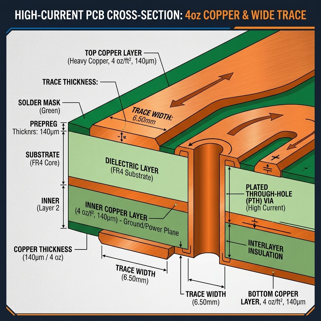
Wählen Sie die Kupferdicke für Ihre Leiterplattenlage aus. Bei Standardplatinen werden 1 oz/ft² verwendet (was einer Dicke von etwa 1,37 mil oder 35 µm entspricht). Bei Hochstrom-Designs verwenden Entwickler häufig 2 oz/ft², 3 oz/ft² oder sogar noch dickeres Kupfer. Dickeres Kupfer bedeutet bei gleicher Leiterbahnbreite eine größere Querschnittsfläche, wodurch Sie mehr Strom auf einer kleineren horizontalen Fläche leiten können.
Schritt 4: Verwenden Sie die IPC-2221-Formel
Setzen Sie Ihren Strom und den zulässigen Temperaturanstieg in die IPC-2221-Formel ein, um die erforderliche Querschnittsfläche zu berechnen. Alternativ können Sie einen der vielen kostenlosen Online-Rechner für Leiterbahnbreiten nutzen, die diese Formel automatisch anwenden und so manuelle Rechenfehler vermeiden.
Schritt 5: Berechnen Sie die endgültige Breite
Sobald Sie die erforderliche Querschnittsfläche (A) ermittelt haben, dividieren Sie diese durch die Kupferdicke (t) der von Ihnen gewählten Schicht, um die minimale Leiterbahnbreite (W) zu ermitteln.
W = A / t
Achten Sie darauf, dass Ihre Einheiten einheitlich sind (z. B. Fläche in Quadratmil, Dicke in Mil, resultierende Breite in Mil).

Praktische Überlegungen zu Schaltungslayouts für hohe Stromstärken
Der IPC-2221-Rechner bietet zwar eine solide Grundlage, doch beim praktischen Leiterplattenentwurf müssen weitere praktische Faktoren berücksichtigt werden.
Verwenden Sie Kupfergießen und Polygone: Bei sehr hohen Strömen (z. B. über 10 A oder 20 A) werden einfache Leiterbahnen unpraktisch breit. Anstatt eine breite Leiterbahn zu verlegen, sollten Sie Kupferpolygone oder durchgehende Ebenen verwenden, um Knoten mit hohem Strom zu verbinden. Dadurch wird die Kupferfläche maximiert, was den Widerstand drastisch senkt und die Wärmeableitung verbessert.
Thermische Entlastungen: Beim Anschließen von Komponenten an große, Hochstrombahnen, verwende Wärmeentlastung Pads. Ohne thermische Entlastungen wirkt die massive Kupferfläche beim Löten als Kühlkörper, wodurch es sehr schwierig wird, die Lötstelle ausreichend zu erwärmen, um eine ordnungsgemäße Lötverbindung herzustellen, was zu kalten Lötstellen und möglichen Ausfällen führt.
Durchkontaktierungen zur Stromführung: Wenn ein hoher Strom von einer Schicht in eine andere geleitet werden muss, reicht eine einzige Durchkontaktierung selten aus. Sie müssen die Strombelastbarkeit der Durchkontaktierung auf der Grundlage ihrer Bohrergröße und die Schichtdicke. Oftmals ist es erforderlich, eine Anordnung aus mehreren Durchkontaktierungen (Via-Stitching) zu verwenden, um hohe Ströme sicher und ohne übermäßige Erwärmung zwischen den Schichten zu leiten.
Halten Sie die Traces kurz: Der Gesamtwiderstand einer Leiterbahn ist proportional zu ihrer Länge. Um Spannungsabfall und Verlustleistung zu minimieren, sollten Hochstrom-Leiterbahnen so kurz und direkt wie möglich gehalten werden. Die Anordnung der Bauteile ist entscheidend; gruppieren Sie Leistungsbauteile dicht beieinander, um die Verlegungswege zu minimieren.
Schlussfolgerung
Die genaue Berechnung der Leiterbahnbreiten auf Leiterplatten für Hochstromanwendungen ist nicht nur eine bewährte Vorgehensweise, sondern eine grundlegende Voraussetzung für Sicherheit und Zuverlässigkeit. Durch das Verständnis des Zusammenhangs zwischen Strom, Widerstand, Kupferdicke und Temperaturanstieg sowie durch die Anwendung von Normen wie IPC-2221 können Entwickler sicherstellen, dass ihre Leiterplatten hohe Leistungen problemlos bewältigen. Denken Sie stets daran, für Worst-Case-Szenarien zu entwerfen, erwägen Sie bei extremen Strömen die Verwendung von dickerem Kupfer oder Polygon-Füllungen und unterschätzen Sie niemals die Bedeutung des Wärmemanagements beim Design von Leistungselektronik.
Häufig gestellte Fragen
Was passiert, wenn eine Leiterbahn auf einer Leiterplatte für hohe Stromstärken zu schmal ist?
Ist eine Leiterbahn auf einer Leiterplatte für den durch sie fließenden Strom zu schmal, führt ihr Widerstand dazu, dass Leistung in Form von Wärme abgegeben wird. Übersteigt die erzeugte Wärme die Kühlleistung, steigt die Temperatur der Leiterbahn an, was zu einer Beschädigung des Leiterplattensubstrats, einer Ablösung des Kupfers oder einem Brand führen kann.
Hat die Kupferdicke Einfluss auf die erforderliche Leiterbahnbreite?
Ja, dickeres Kupfer (z. B. 2 oz oder 3 oz) ermöglicht schmalere Leiterbahnen, da die Gesamtquerschnittsfläche maßgeblich die Strombelastbarkeit bestimmt. Je dicker das Kupfer ist, desto weniger Breite benötigen Sie, um dieselbe Fläche zu erreichen.
Unterscheiden sich die inneren Schichten bei der Berechnung der Leiterbahnbreite von den äußeren Schichten?
Ja, Leiterbahnen auf inneren Schichten erfordern bei gleichem Strom eine größere Breite als Leiterbahnen auf äußeren Schichten. Das liegt daran, dass innere Schichten durch FR4 oder andere Substratmaterialien isoliert sind, wodurch sich Wärme staut, während äußere Schichten die Wärme effizienter an die Umgebungsluft abgeben können.